As the demand for precise control in industrial processes continues to rise, traditional Pulse-Width Modulation (PWM) technology struggles to meet the requirements for high dynamic performance and low harmonic distortion. In contrast, high-frequency PWM technology enhances output waveform quality and reduces system harmonics by increasing the carrier frequency, thereby optimizing the performance of inverters. Consequently, balancing system efficiency and reliability when applying high-frequency PWM technology has become a critical aspect of inverter technology development.
1. Basic Theory and Technical Characteristics of High-Frequency PWM
PWM technology is the core technique used in the electrical control systems of inverters to regulate voltage and frequency. It generates pulse sequences by comparing reference signals with carrier signals and uses these pulse sequences to control the switching states of power devices, thus achieving precise control over power supply to the load. In inverter control, the duty cycle D of PWM can be expressed in relation to the reference wave amplitude Vref and the carrier wave amplitude Vtri as follows:

The modulation ratio m is defined as the ratio of the reference wave amplitude to the carrier wave amplitude. It directly influences the effective value and harmonic characteristics of the output voltage. The expression for this ratio is:

The carrier frequency fc refers to the frequency of the triangular wave used to generate the PWM signal. Its value directly affects the system's dynamic response speed and the distribution of output harmonics. The frequency ratio N is defined as the ratio of the carrier frequency to the reference wave frequency, expressed as:

where is the reference wave frequency. High-frequency PWM technology generally refers to PWM control techniques with a carrier frequency exceeding 10 kHz. In modern inverters, with continuous improvements in power device performance, carrier frequencies have reached 20 kHz or even higher. By increasing the carrier frequency, the output harmonic components are shifted to higher frequency ranges, facilitating subsequent filtering and effectively reducing motor noise and vibration.
Experiments show that increasing the carrier frequency from 5 kHz to 20 kHz can reduce motor noise by 12–15 dB and lower temperature rise by 5–8 °C. As the carrier frequency increases, the PWM output waveform more closely approximates an ideal sine wave, and the Total Harmonic Distortion (THD) is significantly reduced. At a carrier frequency of 20 kHz, the THD of the inverter output voltage drops to approximately 5%, which is considerably better than the 8%–12% typical of low-frequency PWM techniques. Furthermore, high-frequency PWM offers advantages such as faster dynamic response and higher control accuracy.
2. Key Challenges in Implementing High-Frequency PWM and Their Solutions
2.1 High Switching Losses and Mitigation Methods
The most prominent issue with high-frequency PWM technology is the sharp increase in switching losses. Since the switching losses of power devices are proportional to the switching frequency, high-frequency operation leads to reduced system efficiency and increased demands on thermal management. The switching loss Psw of a single Insulated-Gate Bipolar Transistor (IGBT) module can be modeled as follows:

where and are the turn-on and turn-off energy losses, respectively; Err is the reverse recovery energy; Vdc is the actual DC bus voltage; is the reference voltage; is the actual current; and Iref is the reference current.
To suppress switching losses, the following measures can be adopted:
First, use advanced power devices such as Silicon Carbide Metal-Oxide-Semiconductor Field-Effect Transistors (SiC MOSFETs), which offer superior switching characteristics compared to conventional IGBTs;
Second, optimize the gate driver circuit design by employing dual-slope drive techniques to dynamically adjust the gate resistance during switching transitions, thereby balancing switching speed and electromagnetic interference (EMI);
Finally, implement soft-switching techniques, such as zero-voltage switching (ZVS) or zero-current switching (ZCS) topologies, to significantly reduce switching losses.
2.2 Dead-Time Effect and Compensation Techniques
Under high-frequency PWM operation, although the absolute dead-time remains constant, its proportion relative to the switching period increases, making the dead-time effect more pronounced. This can lead to output voltage distortion, degraded low-speed performance, and increased torque ripple. To effectively mitigate these issues, dead-time compensation algorithms are employed, expressed as:
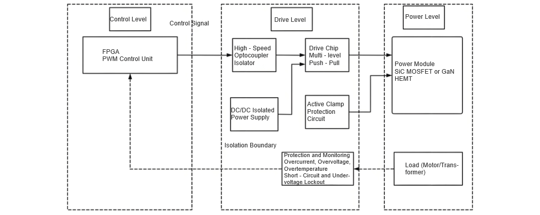
3 FPGA-Based Implementation Scheme for High-Frequency PWM Technology
3.1 System Architecture Design
High-frequency PWM control imposes higher demands on the real-time performance and control precision of computing platforms. Traditional Digital Signal Processors (DSPs) often face limitations such as insufficient computational power and significant interrupt latency when implementing high-frequency PWM. In contrast, Field-Programmable Gate Arrays (FPGAs) are better suited for such applications due to their parallel processing capabilities and hardware-level implementation flexibility.
The overall architecture of the FPGA-based high-frequency PWM control system consists of four core modules: the main control unit, the PWM generation unit, the feedback signal processing unit, and the protection unit. Specifically:
Main Control Unit: Executes closed-loop control algorithms such as speed, current, and position loops;
PWM Generation Unit: Responsible for generating high-precision PWM waveforms and managing dead-time control;
Feedback Signal Processing Unit: Handles the acquisition and preprocessing of signals such as current, voltage, and position;
Protection Unit: Detects and responds to faults such as overcurrent, overvoltage, and overtemperature to ensure system safety.
The system adopts a modular design, with functional modules interconnected via standardized interfaces. Internally, the FPGA employs a dual-clock-domain architecture: control algorithms operate in a lower-frequency clock domain to reduce resource consumption, while the PWM generation module runs in a high-frequency clock domain to ensure precise timing and high resolution.
3.2 Optimization and Implementation of PWM Control Algorithm
To achieve high-performance high-frequency PWM control, the conventional Space Vector Pulse Width Modulation (SVPWM) algorithm is optimized by introducing an improved PWM control algorithm, expressed as:

where Ta is the conduction time of the upper leg of Phase A; vα and vβ are the components of the reference voltage in the α-β coordinate system. This algorithm is implemented in the FPGA using a pipelined architecture, transforming complex trigonometric computations into simple linear operations. This significantly reduces computational latency and enables single-cycle execution. To optimize dead-time control, an adaptive dead-time compensation strategy is adopted.
3.3 System Performance Testing and Analysis
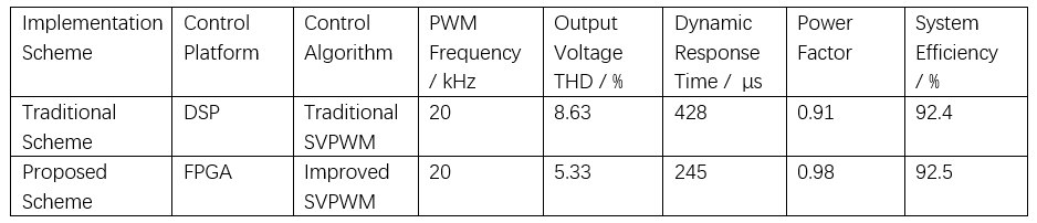
To evaluate the superiority of the proposed high-frequency PWM implementation scheme (hereinafter referred to as the "proposed scheme"), it is compared with a conventional DSP-based implementation (hereinafter referred to as the "conventional scheme"). The test platform is built on a Xilinx Artix-7 FPGA and a TMS320F28379D DSP, using identical power-level circuit topologies and power modules (1200 V/50 A SiC MOSFET). Performance metrics include output voltage Total Harmonic Distortion (THD), dynamic response time, power factor, and system efficiency. Each test is repeated three times, with results averaged to ensure reliability.
As shown in Table 1, the proposed scheme demonstrates significant advantages over the conventional scheme across most metrics: output voltage THD is reduced from 8.63% to 5.33%, a 38.2% improvement; dynamic response time decreases from 428 μs to 245 μs, a 42.5% reduction; and power factor increases from 0.91 to 0.98. Although the system efficiency improves by only 0.1%, this marginal gain is still meaningful given the already high baseline efficiency exceeding 92%.
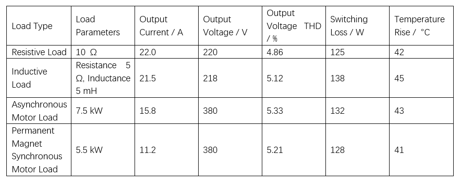
The feasibility of the proposed scheme under varying load conditions is further tested, with results presented in Table 2. The tests cover resistive, inductive, and motor loads. The results show that the proposed scheme maintains stable performance across all load types: the variation in output voltage THD is only 0.47%, demonstrating excellent robustness of the control algorithm; switching losses are maintained between 125 W and 138 W, with a fluctuation of just 10.4%, indicating effective power management; and temperature rise is kept within 41–45 °C, confirming superior thermal stability.
4 Conclusion
High-frequency PWM technology is a key enabler for enhancing inverter performance, yet its implementation in electrical control systems faces multiple technical challenges. This paper addresses critical issues such as high-frequency switching losses, dead-time effects, and driver circuit design by proposing systematic solutions and presenting an FPGA-based implementation framework.
The proposed scheme offers high precision, low latency, and strong real-time performance, effectively improving both dynamic response and steady-state accuracy. The research provides solid technical support for high-performance inverter control and holds broad application potential in fields such as industrial automation, renewable energy generation, and electric vehicles.