
Moore’s Law jiġifiera l-osservazzjoni li d-daqs tal-transistors f’kull integrated circuit (IC) jiżdub approssimativament kull sena tat-tnejn. Huwa sovent qitba bħala spiegazzjoni għall-iżbord tas-silġ tas-teknoloġija, dawn il-kulħadd jinsabu jgħidu li huwa l-‘leggi tas-silġ esponenzjali’.
Moore’s law huwa msemmin wara Gordon Moore, l-assistent fondatur ta’ Intel. Moore osservà li minn meta inventa l-integrated circuits, id-daqs tal-transistors jiżdub kull sena. Moore ipprodusa artiklu fil-magazzin ‘Electronics’ intitolat ‘Cramming More Components Onto Integrated Circuits’ spiegand is-silġ tiegħu (source). Wara ma saret noti, din it-tqies setta tittieles hemm fil-industri elettronika u saret magħrufa bħala Moore’s Law.
Dan is-silġ ħtieg jagħmel kontinwament, jekk mhux jiżdied. L-ispazju fis-sema tagħha kien qasir imma setgħet tkun qasira konstant. Origiナルメッセージの続きを翻訳します。
```html
Originally, Moore predicted that the number of transistors in an IC would double every year. In 1975 Gordon Moore’s prediction was revised at the International Electron Devices Meeting. It was determined that after the year 1980, it would slow down to doubling every two years. The extrapolation of this data has been used in the semiconductor industry for many years to direct long-term planning and set targets for research and advancement. From your laptop, your camera and your phone – any digital electronic device is heavily linked to Moore’s Law. Moore’s Law became somewhat of a goal for the industry to reach, ensuring timely progression in technology. Society has benefited greatly from this advancement in all areas, such as education, health, 3D printing, drones, and much more. We can now do things with beginner Arduino starter kits that 30 years ago could only be performed by expensive mega-computers. At the 1975 IEEE International Electron Devices Meeting, Moore outlined several factors he believed were contributing to this exponential growth: As techniques improved, the potential for defects has dramatically decreased. This combined with an exponential increase in die sizes meant that chip manufacturers could work with larger areas without losing reduction yields Development of the smallest dimensions achievable Conserving space on a circuit is known as circuit cleverness – optimizing how clever components are arranged and eventually finding the optimum use of space Moore’s Law wouldn’t be viable without a few innovations by scientists and engineers over the years. This is the timeline of the factors that enabled Moore’s Law:
Major Enabling Factors
When
Who
Where
What
Why
1947
John BardeenWalter Brattain
Built first working transistor
1958
Jack Kilby
Texas Instruments
Patented the principle of integration and created the first prototype of an integrated circuit and commercialized them
Kurt Lehovec
Sprague Electric Company
Invented a way to isolate components on a semiconductor
Robert Noyce
Fairchild Semiconductor
Created a way to connect components on an IC by aluminum metallization
Jean Hoerni
Planar technology based the improved version of insulation
1960
Group of Jay Last’s
Fairchild Semiconductor
Made the first operational semiconductor integrated circuit
1963
Frank Wanlass
Frank Wanlass
Invented complementary metal-oxide-semiconductor (CMOS)Allowed extremely dense and high-performance IC’s
1967
Robert Dennard
IBM
Created dynamic random-access memory (DRAM)
Enabled the possibility of fabricating single transistor memory cells (led to the invention of flash memory by Fujio Masuoka from in the ’80s allowing low-cost high capacity memory in many devices)
1980
Hiroshi ItoC Grant Wilson J. M. J. Frechet
Agħti tipp u inkoraġixxi l-awtur!
Rigward l-esperji
0
China
Mħalless
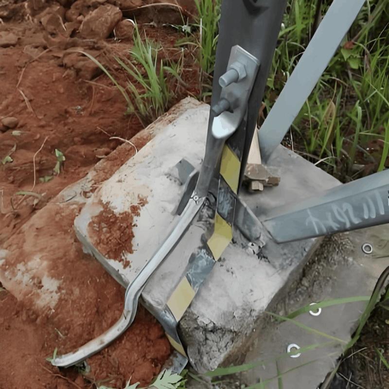 Imbax tal-Voltiġġ: Fattal tal-Terra, Linja Mogħliqa, jew Risonanza?
Il-ġrounding ta' fazzjoni wahda, il-kutur tal-linja (open-phase), u r-risonanza jistgħu kollha jiġġibu disiġna fil-volttagġ tat-tliet fazzjonijiet. Tiftix sewwa bejnhom huwa essenzjali għal t-troubleshooting veloċi.Il-Ġrounding ta' Fazzjoni WahdaAnki l-ġrounding ta' fazzjoni wahda jiġġib disiġna fil-volttagġ tat-tliet fazzjonijiet, il-magnitudo tal-volttagġ linja-linja jirriman mhux maġbula. Tista' tkun klassifikata fi żewġ tipi: grounding metaliku u grounding mhux metaliku. Fil-grounding metali
11/08/2025
Imbax tal-Voltiġġ: Fattal tal-Terra, Linja Mogħliqa, jew Risonanza?
Il-ġrounding ta' fazzjoni wahda, il-kutur tal-linja (open-phase), u r-risonanza jistgħu kollha jiġġibu disiġna fil-volttagġ tat-tliet fazzjonijiet. Tiftix sewwa bejnhom huwa essenzjali għal t-troubleshooting veloċi.Il-Ġrounding ta' Fazzjoni WahdaAnki l-ġrounding ta' fazzjoni wahda jiġġib disiġna fil-volttagġ tat-tliet fazzjonijiet, il-magnitudo tal-volttagġ linja-linja jirriman mhux maġbula. Tista' tkun klassifikata fi żewġ tipi: grounding metaliku u grounding mhux metaliku. Fil-grounding metali
11/08/2025
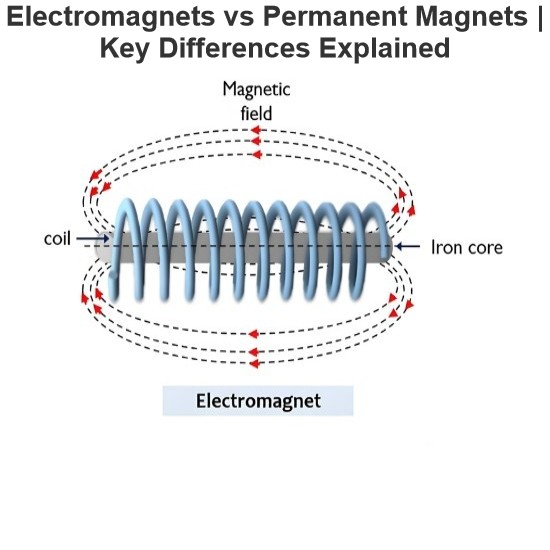 Elettromagneti vs Magneti Permanenti | Spjegati l-Ifferenzi Mhuxxija
Elettromagneti vs. Magneti Permanenti: Spiegazzjoni tal-Differenzi FondamentaliL-elettromagneti u l-magneti permanenti huma l-żewġ tipi primarji ta’ materjal li jipperluħu proprjetajiet magneżki. Anki billi tkun kollox jagħmlu maqsi magneżki, dawn jiżbeddu fundamentali fil-mod kif din il-maqsi tuġġibu.L-elettromagnet għandu maqs maġnetiku biss meta telf huwa jirreġġel fil-kors. Fil-kontrari, l-magnet permanent inqasam automatikament maqs maġnetiku persistenti waqt li huwa mitmummin, mingħajr li
08/26/2025
Elettromagneti vs Magneti Permanenti | Spjegati l-Ifferenzi Mhuxxija
Elettromagneti vs. Magneti Permanenti: Spiegazzjoni tal-Differenzi FondamentaliL-elettromagneti u l-magneti permanenti huma l-żewġ tipi primarji ta’ materjal li jipperluħu proprjetajiet magneżki. Anki billi tkun kollox jagħmlu maqsi magneżki, dawn jiżbeddu fundamentali fil-mod kif din il-maqsi tuġġibu.L-elettromagnet għandu maqs maġnetiku biss meta telf huwa jirreġġel fil-kors. Fil-kontrari, l-magnet permanent inqasam automatikament maqs maġnetiku persistenti waqt li huwa mitmummin, mingħajr li
08/26/2025
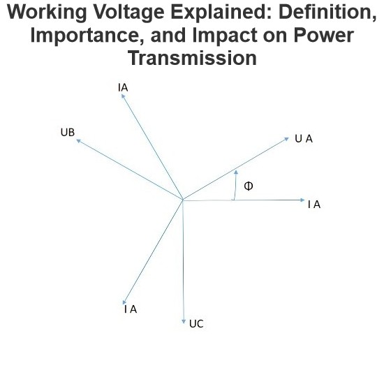 Tensjoni Operattiv Spjegata: Definizzjoni Importanza u Impatt fuq it-Trasferiment tal-Energija Elettrika
Volt tal-GħododIl-term "volt tal-għodod" referi lill-volt massimu li t-togħmir tista’ tisbir mingħajr ma timolli dani jew tiskaddeġ, waqt li tassegura r-relibilta', is-sigurtà, u l-funzjonament korrett tant ta' t-togħmir kif ukoll tas-sistemi assosjati.Għal it-trasferiment tal-enerġija elektrika fuq distanzi lil hinn, l-użu tal-volt għoli huwa avantazzjuż. Fis-sistemi AC, l-iktar ċara possibbli tal-potenzjal tal-karigg huwa wkoll ekonomika neċessarja. Prattika, il-kurrenti qawwi huma aktar diffi
07/26/2025
Tensjoni Operattiv Spjegata: Definizzjoni Importanza u Impatt fuq it-Trasferiment tal-Energija Elettrika
Volt tal-GħododIl-term "volt tal-għodod" referi lill-volt massimu li t-togħmir tista’ tisbir mingħajr ma timolli dani jew tiskaddeġ, waqt li tassegura r-relibilta', is-sigurtà, u l-funzjonament korrett tant ta' t-togħmir kif ukoll tas-sistemi assosjati.Għal it-trasferiment tal-enerġija elektrika fuq distanzi lil hinn, l-użu tal-volt għoli huwa avantazzjuż. Fis-sistemi AC, l-iktar ċara possibbli tal-potenzjal tal-karigg huwa wkoll ekonomika neċessarja. Prattika, il-kurrenti qawwi huma aktar diffi
07/26/2025
 X’huwa l-kirkit AC purament reżistiv?
Ċirkwit Tqassim Aċċessjivi ĠġenunĊirkwit li jilgħab biss reżistanza ġġenuna R (fil-ohmi) f'sistema ta' aċċessjività huwa definit bħala Ċirkwit Tqassim Aċċessjivi Ġġenun, bla induktanza jew kapazzità. Il-kurrent aċċessjiv u l-volttagġ fiċ-ċirkwit dan jiġġġawdu bidirezzjonali, jikkrejaw sinewave (forma sinusoidali). Fi konfigurazzjoni din, il-potenza tkun dissippata mill-rezistor, bil-volttagġ u kurrent fl-faża perfetta — dawn jirragġungu l-valuri massi tagħhom issaħħan. Bil-mezzu passiv, ir
06/02/2025
Ċalja tal-inquery
Downloadu
Ikseb l-App IEE Business
Uża l-app IEE-Business biex tiftakar imkienjar taħt il-mod ġdid waqt li tkun qiegħed tixtieq soluzzjonijiet tikkonektja ma' esperti u tkun parti min kollobazzjoni f'sektor kwalunkwe ħin u fejn siekta s-sodisfaċċament tas-silġ tal-proġetti tiegħek u t-affarijiet tiegħek fl-enerġija
X’huwa l-kirkit AC purament reżistiv?
Ċirkwit Tqassim Aċċessjivi ĠġenunĊirkwit li jilgħab biss reżistanza ġġenuna R (fil-ohmi) f'sistema ta' aċċessjività huwa definit bħala Ċirkwit Tqassim Aċċessjivi Ġġenun, bla induktanza jew kapazzità. Il-kurrent aċċessjiv u l-volttagġ fiċ-ċirkwit dan jiġġġawdu bidirezzjonali, jikkrejaw sinewave (forma sinusoidali). Fi konfigurazzjoni din, il-potenza tkun dissippata mill-rezistor, bil-volttagġ u kurrent fl-faża perfetta — dawn jirragġungu l-valuri massi tagħhom issaħħan. Bil-mezzu passiv, ir
06/02/2025
Ċalja tal-inquery
Downloadu
Ikseb l-App IEE Business
Uża l-app IEE-Business biex tiftakar imkienjar taħt il-mod ġdid waqt li tkun qiegħed tixtieq soluzzjonijiet tikkonektja ma' esperti u tkun parti min kollobazzjoni f'sektor kwalunkwe ħin u fejn siekta s-sodisfaċċament tas-silġ tal-proġetti tiegħek u t-affarijiet tiegħek fl-enerġija