• Product
  • Suppliers
  • Manufacturers
  • Solutions
  • Free tools
  • Knowledges
  • Experts
  • Communities
Search


Why Solid-State Transformers (SST) Rely Heavily on SiC/GaN Wide-Bandgap Devices?

RW Energy
Field: Distribution Automation
10Year<
China
 

The Bottleneck of Traditional Silicon-Based Devices

The core operating principle of a Solid-State Transformer (SST) is to elevate the traditional power-frequency (50/60 Hz) conversion to medium/high frequency (tens to hundreds of kHz), thereby drastically shrinking the magnetic core volume. Traditional silicon-based IGBTs, constrained by material properties, typically achieve practical switching frequencies below 5 kHz in medium/high-voltage high-power scenarios, and generally not exceeding 20 kHz even in low-voltage applications.

They also suffer from large reverse-recovery losses and slow switching speeds, which fundamentally limit the high-frequency operation and miniaturisation of SSTs.

iee-business

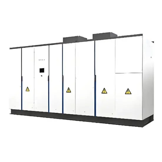
Modular Solid State Transformers for Adaptable Energy Integration

Core Advantages of SiC/GaN Wide-Bandgap Devices

High Voltage & High Frequency Compatibility

  • SiC has a bandgap of 3.26 eV (silicon: 1.1 eV), a critical breakdown electric field strength approximately 10× that of silicon, and a thermal conductivity roughly 3× that of silicon.
  • This enables SiC MOSFETs to operate reliably in medium-voltage (kilovolt-class) environments while supporting switching frequencies of 20 kHz to 100 kHz or higher.

Significantly Reduced Losses

  • SiC MOSFETs exhibit virtually no minority-carrier storage effect; their switching process is primarily limited by parasitic capacitance charging/discharging, eliminating the tail-current problem inherent to IGBTs.
  • In optimised SST designs, system efficiency reaches 96–98.5%, maintained across a wide load range — not just at full load.

Drastic Volume & Weight Reduction

  • Following the inverse relationship between transformer volume and operating frequency (V ∝ 1/f), a 10× frequency increase reduces high-frequency transformer core volume by ~90%.
  • At the system level, SST volume can shrink to one-third or less of a traditional power-frequency transformer, with weight reduced to approximately half.

High-Temperature Capability & Reliability

  • SiC devices operate stably at junction temperatures ≥ 175 °C, offering far superior thermal stability compared to silicon devices — essential for harsh grid-side environments.

SiC vs. GaN: Division of Labour in SST

Two mainstream technology routes coexist in the industry:

SiC Route — High-Power Module Approach (Medium/High Voltage)

  • Targets medium/high-voltage scenarios; commercial SiC MOSFETs now cover 1.7 kV to 15 kV voltage classes
  • Widely used in SST input rectifier stages and high-frequency isolation DAB stages, fitting the cascaded architectures of 10 kV/35 kV medium-voltage grids
  • 2026: commercial 10 kV SiC MOSFETs have entered the market, further reducing series-stack counts and simplifying system architecture

GaN Route — Distributed Small-Power Module Approach (Low Voltage / High Frequency)

  • GaN bandgap ~3.4 eV; breakdown field >10× silicon, supporting MHz-class switching frequencies
  • Commercial single-die voltage ratings mostly ≤ 900 V (typically 650 V)
  • Companies such as Enphase adopt a distributed architecture: many small GaN HEMT modules combined — AC-side series connection for voltage sharing, DC-side parallel connection for current sharing; per-module voltage stress ~300 V, comfortably covered by 650 V GaN devices
  • Advantages: faster response, inherent redundancy, cost efficiency at module level
  • Challenges: higher system-level hardware complexity; multi-module architectures exhibit higher losses under light-load conditions

iee-business

Cost & Industrialisation Context

Power electronic devices account for ≈40% of total SST cost — the single largest cost item.

With the SiC industry transitioning from 6-inch to 8-inch wafers, volume production costs are expected to fall significantly from 2026 onward, further accelerating SST commercialisation.

Application-Driven Demand

Key Scenarios

  • AI Data Centres — single-site power reaching tens to hundreds of MW, cluster power up to GW scale
  • Renewable Integration, Ultra-Fast Charging — emerging applications demanding extreme efficiency and power density

SST Performance Enabled by Wide-Bandgap Devices

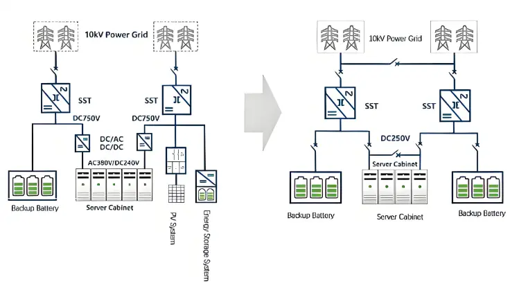
  • Direct conversion of 10–35 kV medium-voltage AC to 800 V high-voltage DC
  • System efficiency up to 98.5%
  • ~60% footprint reduction versus traditional UPS solutions

These performance targets are unattainable without SiC/GaN wide-bandgap devices.

iee-business

Summary

SSTs adopt SiC/GaN wide-bandgap devices en masse because traditional silicon devices hit a ceiling in frequency, efficiency, and volume simultaneously. Wide-bandgap semiconductors, with their wider bandgap, higher breakdown field, and higher thermal conductivity, naturally match the SST's core demands for high frequency, high efficiency, and high power density.

  • SiC dominates medium/high-voltage, high-power segments
  • GaN focuses on low-voltage, high-frequency and distributed small-power module architectures

The two technologies co-operate to cover the full SST chain. Without wide-bandgap semiconductors, the commercialisation of Solid-State Transformers — from laboratory to grid, data centres, and renewable energy applications — would not be possible. They are the key enabling technology.

Edited From:Echo

Give a tip and encourage the author!

Comments

Share your question or perspective
WhatsApp
Send inquiry
+86
Click to upload file
Download
Get the IEE Business Application
Use the IEE-Business app to find equipment, obtain solutions, connect with experts, and participate in industry collaboration anytime, anywhere—fully supporting the development of your power projects and business.
Login
or continue with
New here?
Register