Pêşnûma Bipolar Junction Transistor
Transistor Bipolar Junction (BJT) ji sê terminalan ve hatî ye. Li gorî ku dikeve ya input û output de bikar bîne, divê yek ji terminalan bi du rastîn wekheviyê were bikarber. Vebijarka terminalê ya girîng li ser xebitina were qeyt bike. Sê cûreya pêşnûman transistorean hene: base girîng, emitter girîng, û collector girîng.
Yek ştir li vir ne ku her çi ke pêşnûmana transistorê be, lê girêdanîna base-emitter divê bi vebijarka forward biased re were girîng kirin û girêdanîna base-collector divê bi vebijarka reverse biased re were girîng kirin.
Pêşnûma Base Girîng BJT
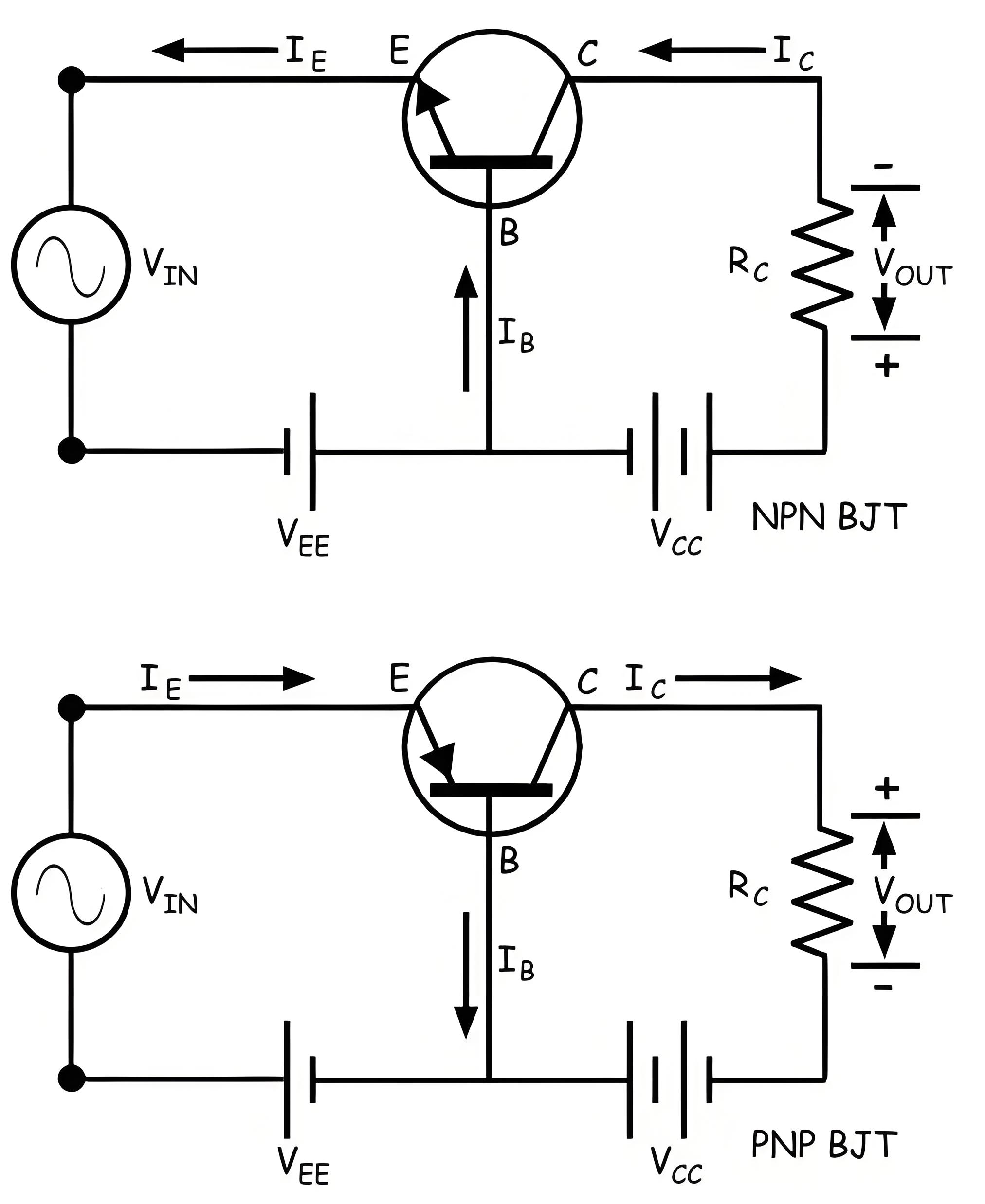
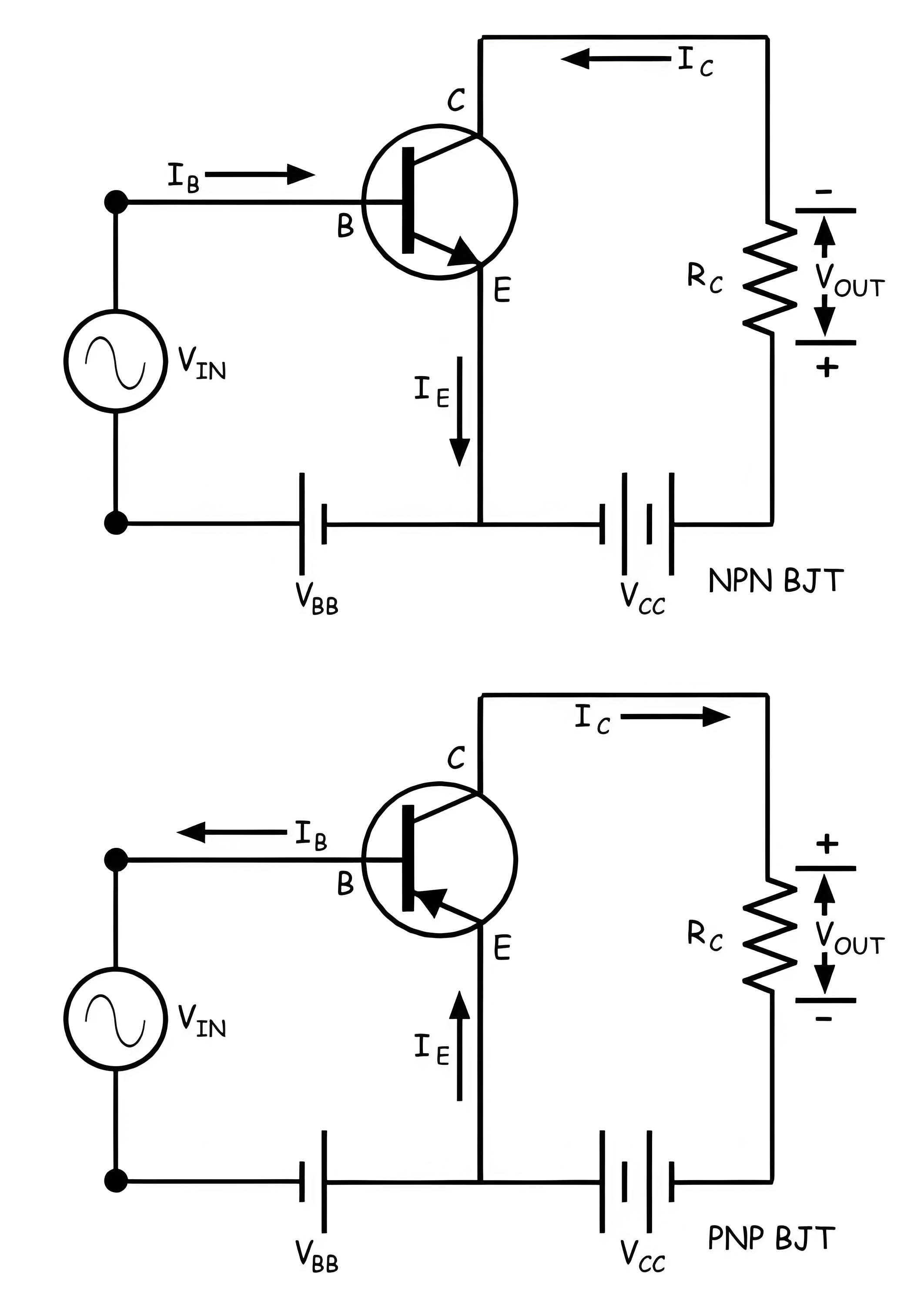
Li vir terminala base li du rastîn wekheviyê yên input û output de girîng e. Pêşnûman base girîng an modes yên npn transistor û pnp transistor li vir wergerandin. Li vir, girêdanîna emitter-base wek circuita input û girêdanîna collector base wek circuita output tayin kirin.

Gewra Gain
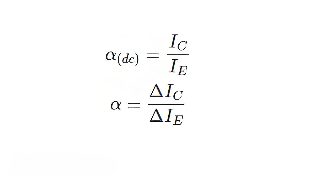
Li vir currenta input IE û currenta output IC e. Gewra gain di dema ku ew jîn dikare bi vebijarkên dc biasing re bînin û tune signal alternating tune nabe di input de. Eger tune signal alternating tune li input de bînin, heqa factora amplification (α) bi voltage collector-base constant re bûyî:
Li vir dîtin ku neherewe gewra gain û factora amplification value yên piştî yekan nabe, chon currenta collector tune nabe piştî currenta emitter. Lê ew zanîn ku currenta emitter û collector yan tune nabe di bipolar junction transistor de, ev ratios yan tune nabe bi yekan. Value generally ranges from 0.9 to even 0.99.

Expression of Collector Current
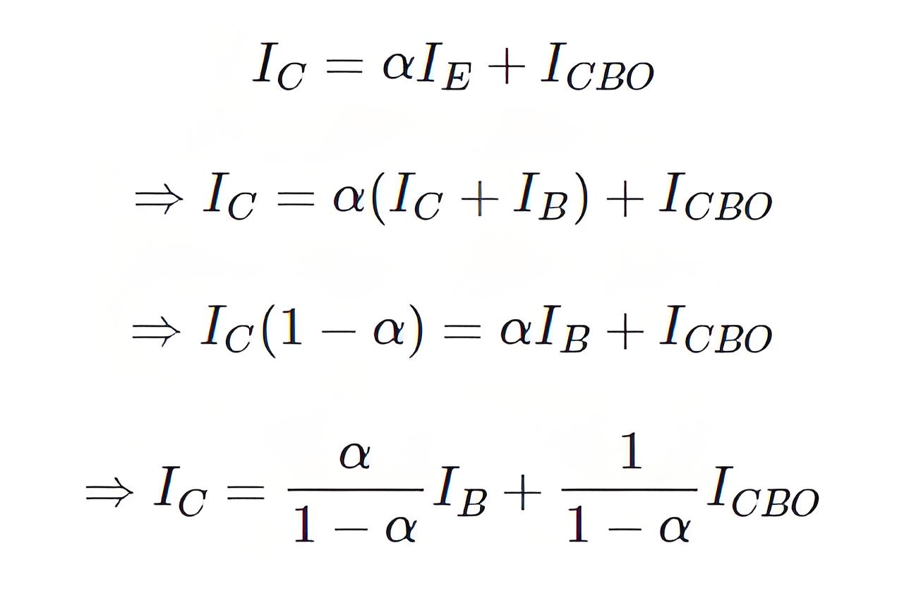
Eger circuita emitter open be, tune nabe currenta emitter (IC = 0). Lê li vir dema, tune nabe currenta bicik li regiona collector da. Ev li ser flow minority charge carriers re ye û ev currenta reverse leakage e. Ji ber ku currenta li vir collector û base dikeve û terminala emitter open be, currenta bi ICBO namek deno. Li small power rated transistor currenta reverse leakage ICBO quite small e û generally, we neglect it during calculations but in high power rated transistor this leakage current cannot be neglected. This current is highly dependent on the temperature so at high temperatures the reverse leakage current ICBO cannot be neglected during calculations. This expression proves that collector current also depends on base current.

Characteristic of Common Base Connection
Input Characteristic
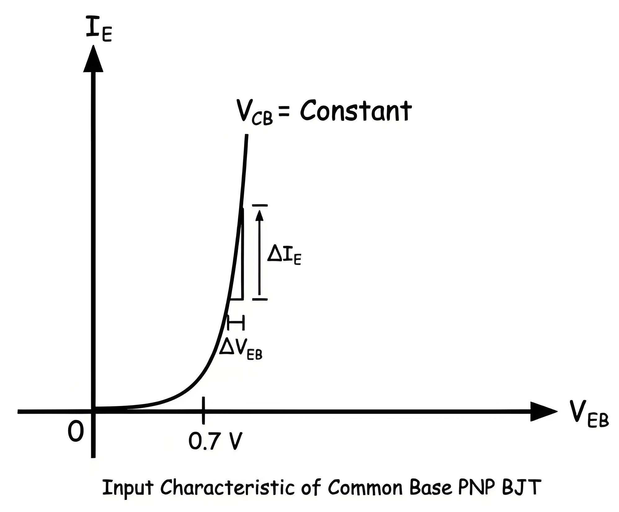
Ev li ser currenta input û voltage input transistor itself re hatine çawn. Currenta input IE û voltage input VEB e. After crossing emitter-base junction forward barrier potential emitter current (IE) starts increasing rapidly with increasing emitter-base voltage (VEB).

The inpur resistance of the circuit is the ratio of change in emitter-base voltage (ΔV EB) to emitter current (ΔIE) at a constant collector-base voltage (VCB = Constant). As the change in emitter current is quite large compared to the change in emitter-base voltage (ΔIE >> ΔVEB), the input resistance of the common base transistor is quite small.

Output Characteristic
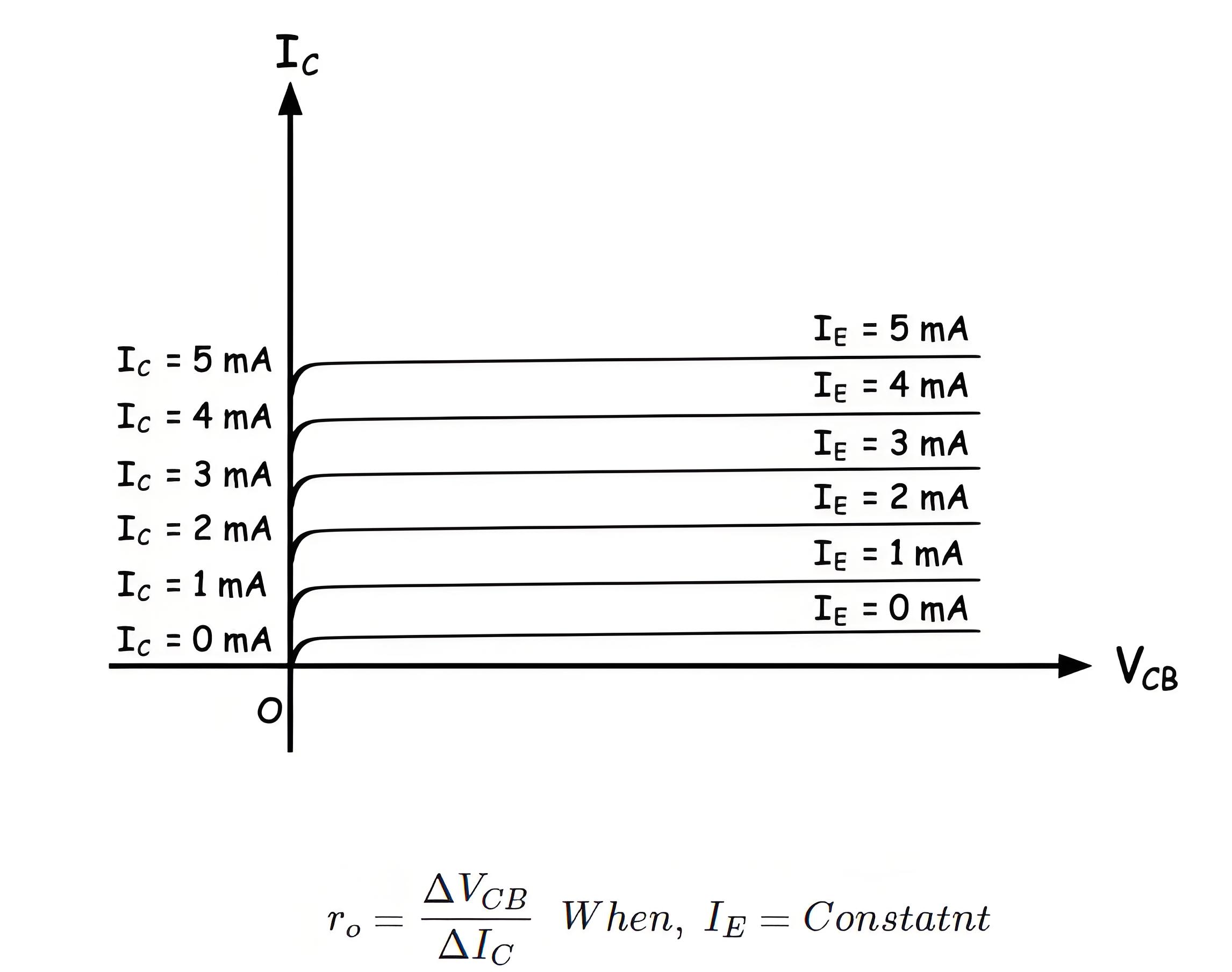
Collector current gets only constant value when there is sufficient reverse biased established between base and collector region. This is why there is a rise of collector current with an increase of collector-base voltage when this voltage has very low value. But after a certain collector-base voltage the collector-base junction gets sufficient reverse biased and hence the collector current becomes constant for a certain emitter current and it entirely depends on the emitter current.
At that situation, the entire emitter current except base current contributes the collector current. As the collector current becomes almost constant for the specified emitter current at that region of the characteristic, the increase of collector current is very very small compared to the increase of collector-base voltage.
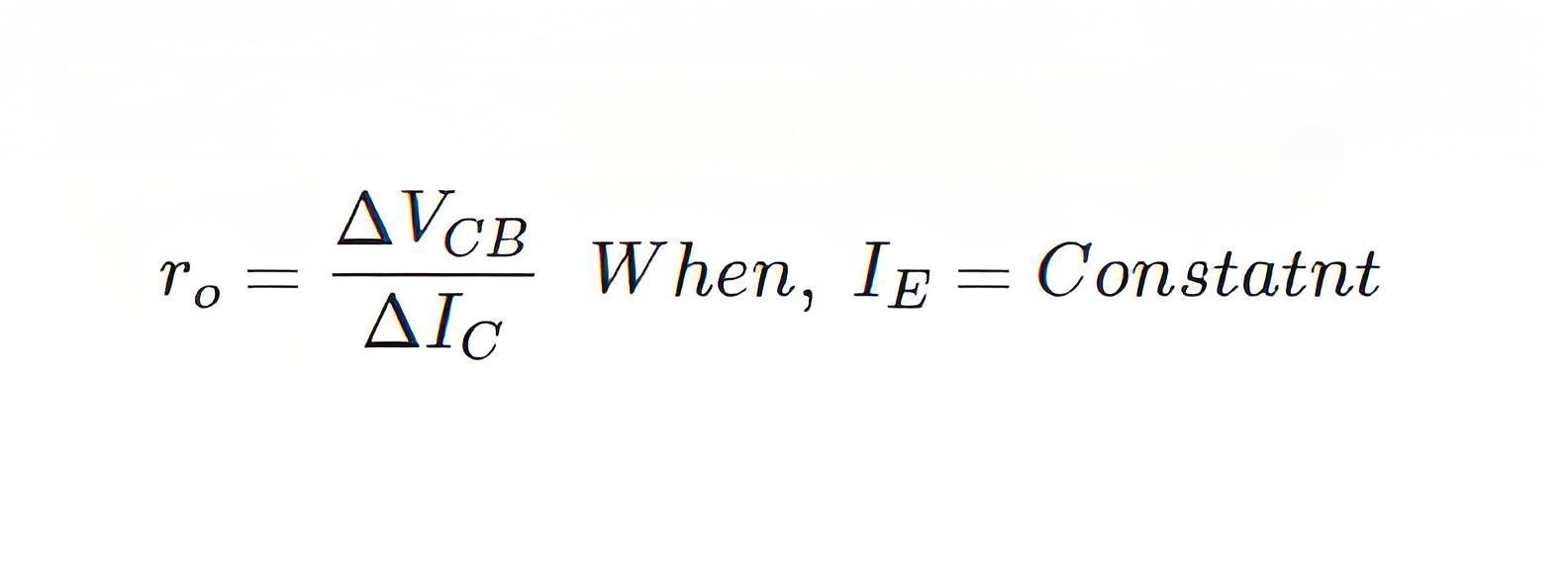
The ratio of change in collector-base voltage to the change in collector current is defined as the output resistance of common base mode of a transistor. Naturally, the value of output resistance is very high in the common base mode of a transistor.

Common Emitter Connection of BJT
Common Emitter Transistor is the most commonly used transistor connection. Here the emitter terminal is common for both input and output circuit. The circuit connected between base and emitter is the input circuit and the circuit connected between collector and emitter is the output circuit. The common emitter mode of npn transistor and pnp transistor are shown separately in the figure below.

Current Gain
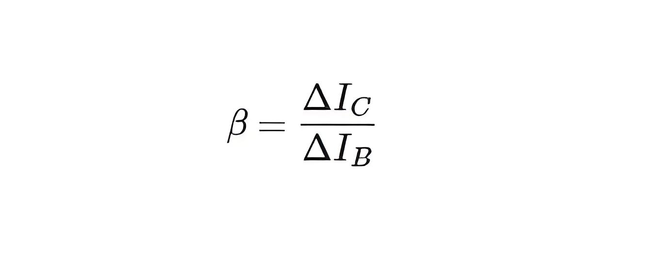
In common emitter configuration, the input current is base current (IB) and the output current is collector current (IC). In bipolar junction transistor, the base current controls the collector current. The ratio of change in collector current (ΔIC) to change in base current (ΔIB) is defined as the current gain of common emitter transistor. In a bipolar junction transistor, the emitter current (IE) is the sum of the base current (IB) and collector current (IC). If base current changes, the collector current also changes and as a result the emitter current gets also changed accordingly.
Again the ratio of change of collector current to the corresponding change in emitter current is denoted by α. As the value of base current is quite low compared to the collector current (IB << IC), the current gain in a common emitter transistor is quite high and it ranges from 20 to 500.

Characteristic of Common Emitter Transistor
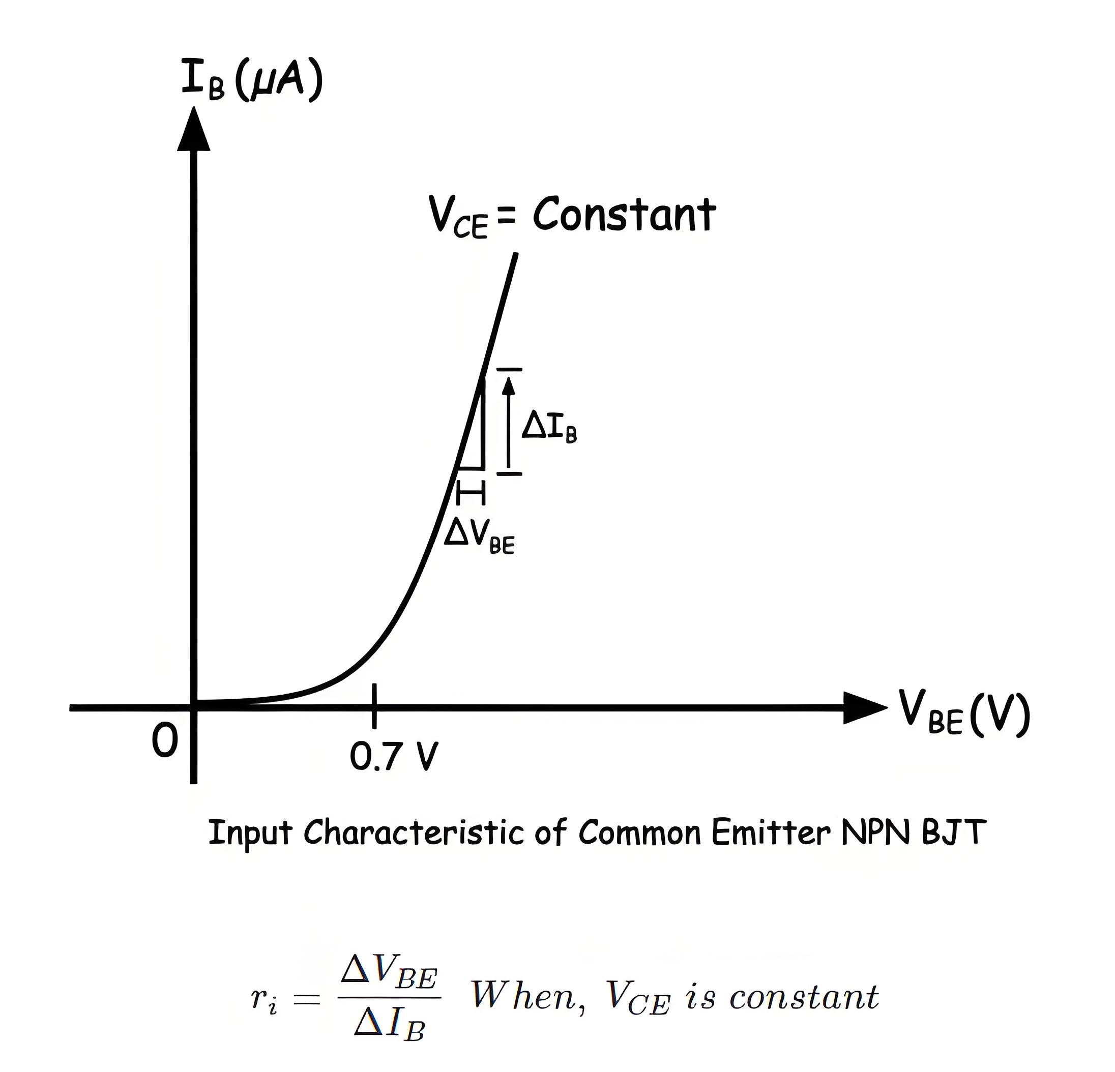
In common emitter mode of the transistor, there are two circuits – input circuit and the output circuit. In the input circuit, the parameters are base current and base-emitter voltage. The characteristic curve drawn against variations of base current and base-emitter voltage is input characteristic of a common emitter transistor. The pn junction between base and emitter is forward biased hence the characteristic would be similar to that of a forward biased pn junction diode. Here also the base current does not get any value before the base-emitter voltage crosses the forward barrier potential of the junction but after that, the base current rises significantly with the increase of base-emitter voltage. The rate of rising of base current with respect to the base-emitter voltage is high here but not as high as in the case of common base mode.
Hence input resistance of the circuit is higher than that of the common base mode of a transistor.

Output Characteristic of Common Emitter Transistor
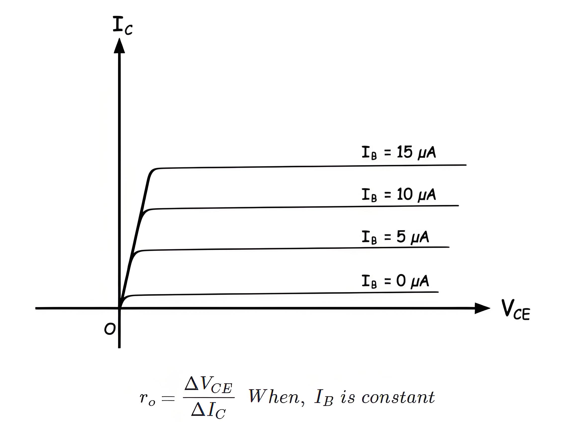
The output characteristic is drawn against variations of output current and the output voltage of the transistor. The collector current is output current and collector-emitter voltage is the output voltage of the transistor. Here the variation of collector current for different values of collector-base voltage is plotted against a fixed value of base current. It is found that at the beginning the collector current proportionately gets increased with increasing collector-emitter voltage but after certain voltage level, the collector current becomes almost constant. This is because at the beginning the base-collector junction does not get sufficient reverse biasing but after a certain voltage it becomes sufficiently reverse biased and then the major portion of charge carriers coming from emitter region to base region would migrate to collector region to contribute collector current. The number of majority carriers coming from emitter region depends on the base current in a BJT hence for a specific base current the collector current is constant.
The output resistance would be

Common Collector Connection of BJT
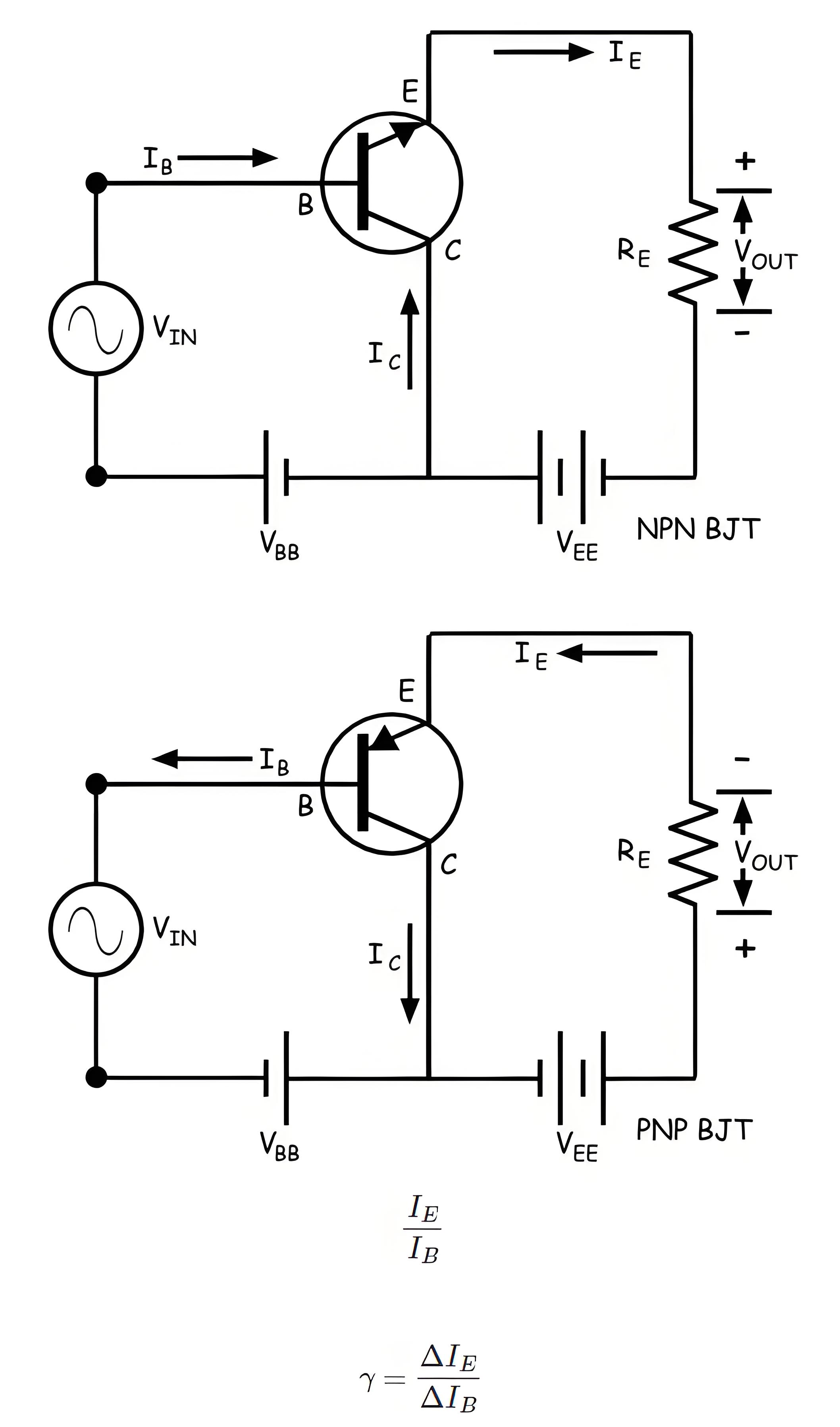
In common collector configuration the input circuit is between base and collector terminal and the output circuit is between emitter and collector terminal.
The ratio of change of emitter current to change of base current is defined as the current gain of common collector configuration. This is denoted as,
The current amplification factor of the circuit is the ratio of change of emitter current to change of base current when a time-varying signal is applied to the input.

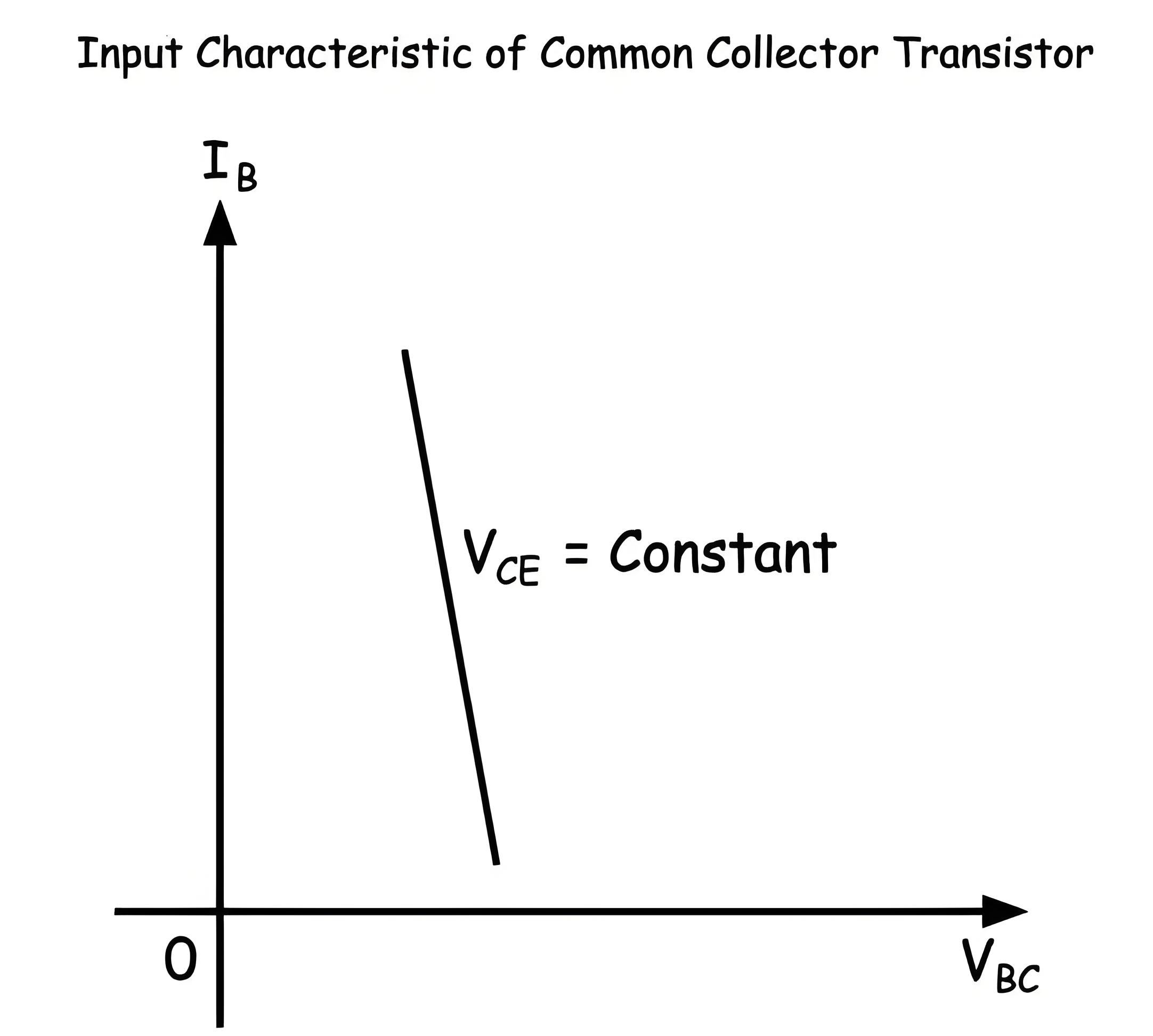
Input Characteristic of Common Collector Transistor
The input current is base current and input voltage of the transistor is base-collector voltage. The base-collector junction is reverse biased and hence with increasing base-collector voltage the reverse biasing of the junction increases. This causes base current to decrease slightly with the increase in base-collector voltage. Since at this condition more minority carriers of the base region will propagate to collector region and hence electron-hole recombination rate would get decreased in the base region causing a decrement in base current.

Output Characteristic of Common Collector Transistor
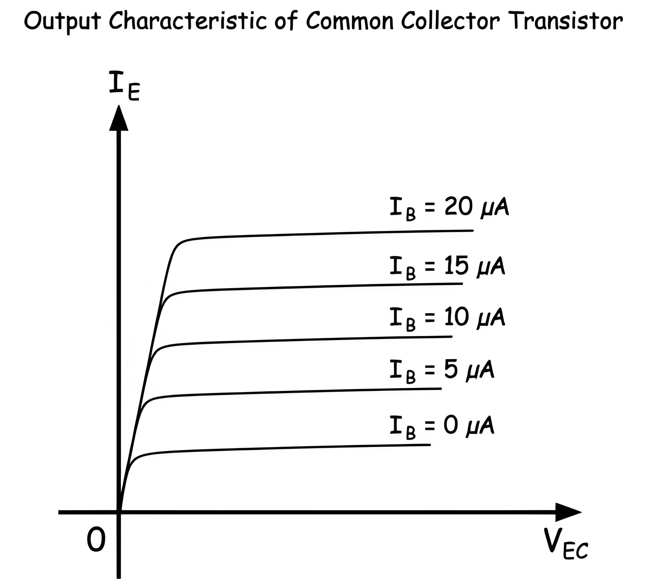
The output characteristic of a common collector transistor is nearly the same as the output characteristic of a common emitter transistor. The only difference that here in the case of common collector configuration the output current is emitter current instead of collector current as in the case of common emitter configuration. Here also for a fixed base current, the emitter current increases linearly with increasing collector-emitter voltage up to a certain level of this voltage and then the emitter current gets almost constant irrespective of collector-emitter voltage. Although there would be a very slow increase of emitter current with the collector-emitter voltage as shown in the characteristic curve below.
