Takaitaccen Bipolar Junction Transistor
Bipolar Junction Transistor (BJT) shine tufafin faduwar da yake da sauran maza. Ana iya amfani da shi a matsayin takamawa ko kuma karamin sakamako, ana bukata sabon tufa na gida da tufa na fitarwa. Don haka za su iya yi waɗannan abubuwa game da maza uku, ya zama cewa wanda daga cikinsu ne ke jirgin da take da sabon tufa da tufa na fitarwa. Zan iya zaba wannan tufa mai girma ta hanyar muhimmin addini. Akwai nau'o'i uku na takamatar transistor: common base, common emitter, da common collector.
A nan akwai wani abu da ya kamata a rike cewa babu wani abun da aka ƙare da transistor, amma ya kamata a duba cewa junction base-emitter ya zama forward biased da kuma junction base-collector ya zama reverse biased.
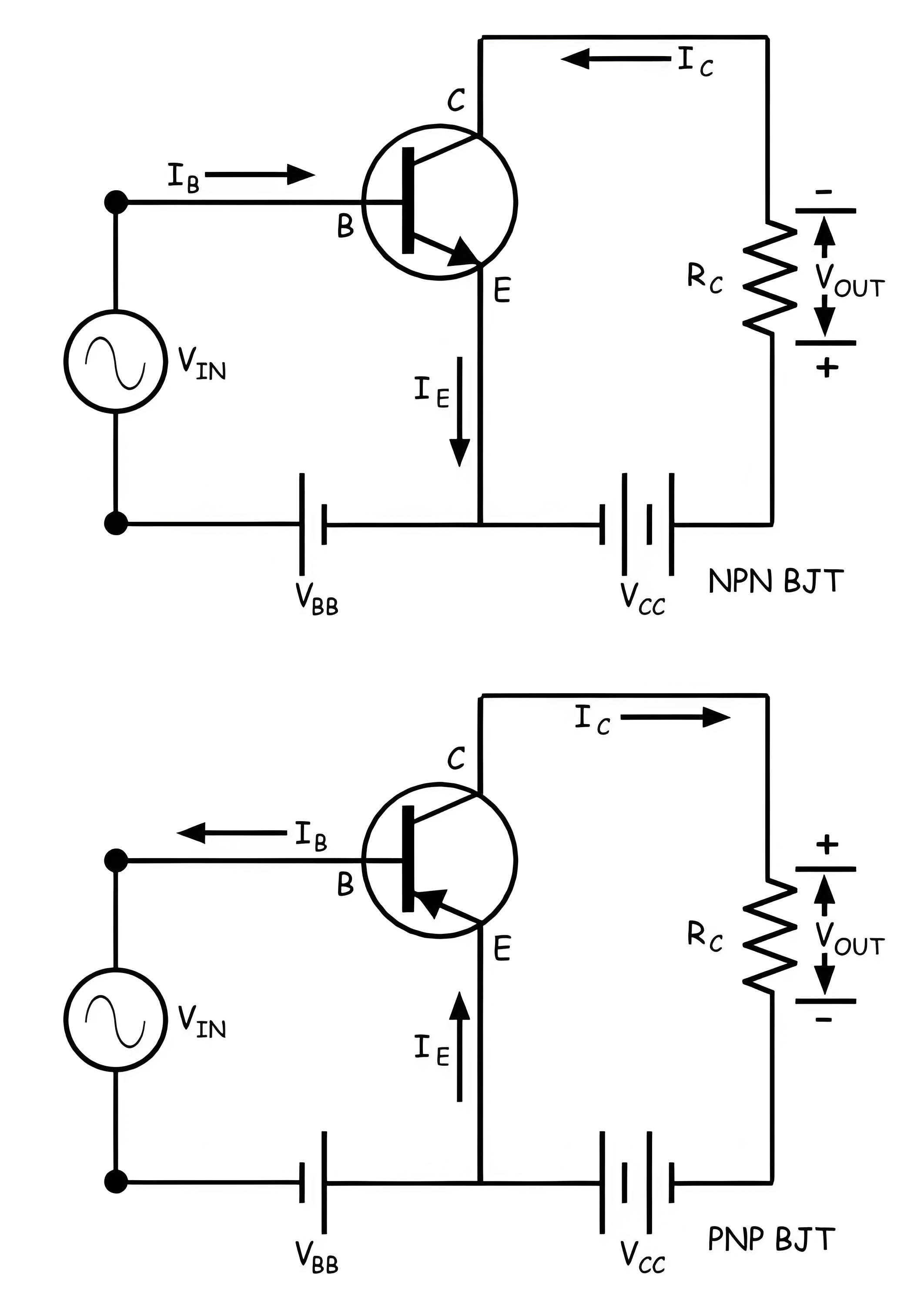
Common Base Connection of BJT
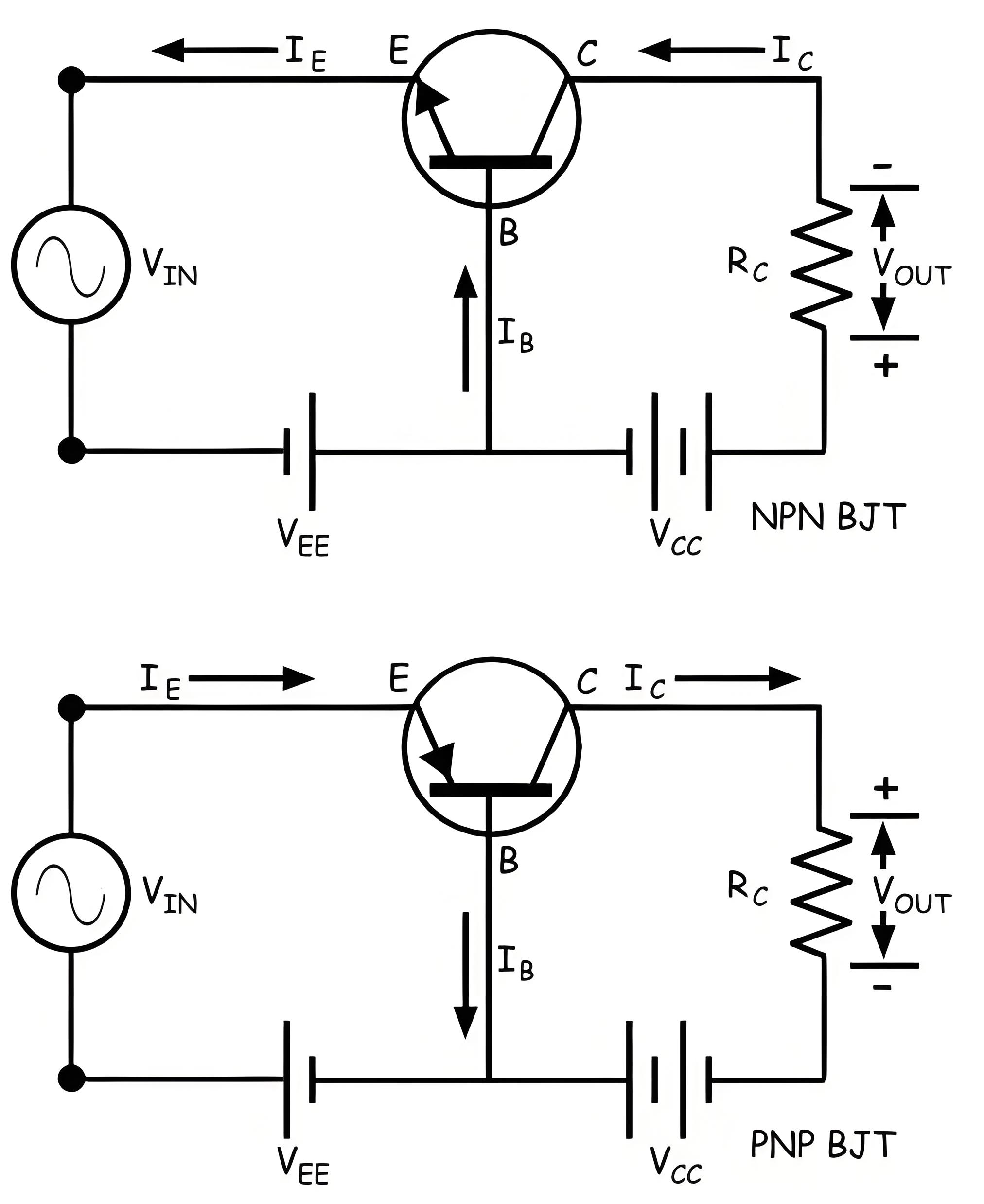
A nan tufa mai girma shine tufa mai girma ga sabon tufa da tufa na fitarwa. Wannan tushen common base configurations ko modes suna nufin cewa an samu a cikin hotunan da ake bayyana a nan. A nan an nuna tushen common base mode na npn transistor da pnp transistor a gaban-gaban. A nan tufa mai girma shine tufa mai girma, amma tufa mai girma shine tufa mai girma.

Current Gain
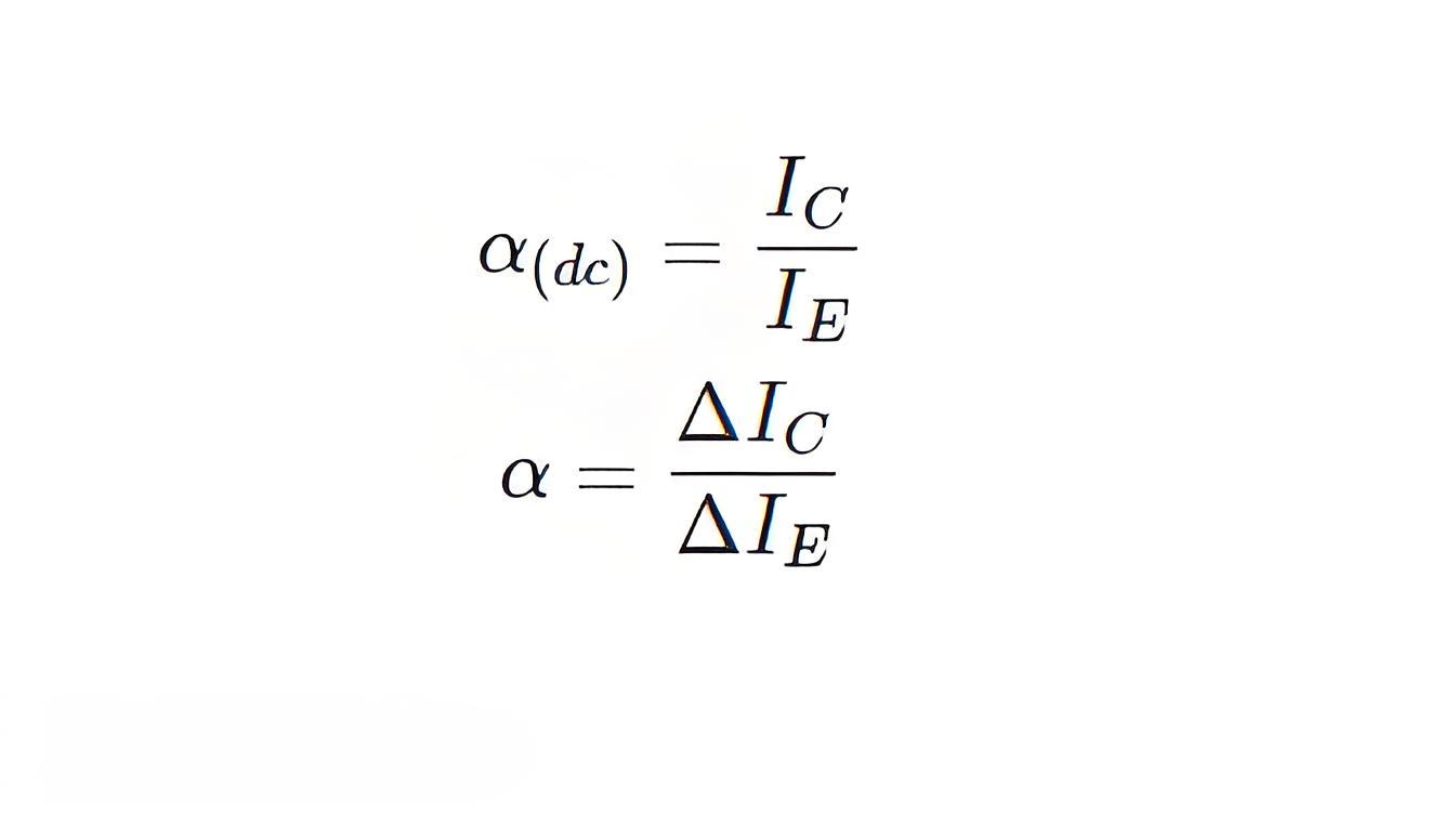
A nan tufa mai girma shine tufa mai girma, da kuma tufa mai fitarwa shine tufa mai fitarwa. Tufa mai girma ya kasance idan muna duba cewa a nan muna bi ɗaya da biasing voltages na dc kawai, ba muna bi wani alternating signal a sabon tufa. Idan muna bi alternating signal a sabon tufa, ya zama cewa current amplification factor (α) a cikin voltage constant collector-base, ya zama
A nan an samu cewa bane tufa mai girma ko current amplification factor ba suka da ma'ana da ya fi yawa unity, saboda tufa mai fitarwa ba za su iya fi yawa tufa mai girma. Amma a nan muna sani cewa tufa mai girma da tufa mai fitarwa suna da damar sama a cikin bipolar junction transistor, wannan ratio ya zama da damar sama da unity. Ma'ana ta zama tare da 0.9 zuwa 0.99.

Expression of Collector Current
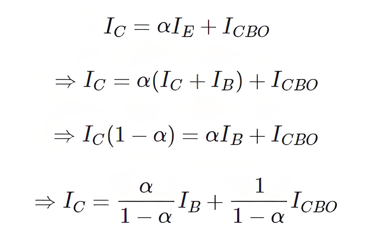
Idan tufa mai girma ya zama open, bai zama tufa mai girma (IC = 0). Amma a cikin wannan halin, za a iya samun tufa mai girma mai tsarki a cikin tufa mai fitarwa. Wannan shine saboda flow of minority charge carriers, kuma wannan shine tufa mai girma mai tsarki. Saboda wannan tufa ya haɗa a cikin tufa mai fitarwa da tufa mai girma, a kan tufa mai girma, wannan tufa ya zama ICBO. A nan transistor da power rating mai tsawo, tufa mai girma mai tsarki ICBO shine mai tsawo, amma a nan muna tafiya shi a lokacin masana'antu. Duk da haka a transistor da power rating mai yawa, ba muna iya tafiya shi, saboda tufa mai girma mai tsarki ICBO ya zama mai yawa a fannoni mai yawa. Wannan tufa shine mai karanci ga temperature, saboda a fannoni mai yawa, tufa mai girma mai tsarki ICBO ba muna iya tafiya shi a lokacin masana'antu. Wannan expression ya nuna cewa tufa mai fitarwa ya zama da tufa mai girma.

Characteristic of Common Base Connection
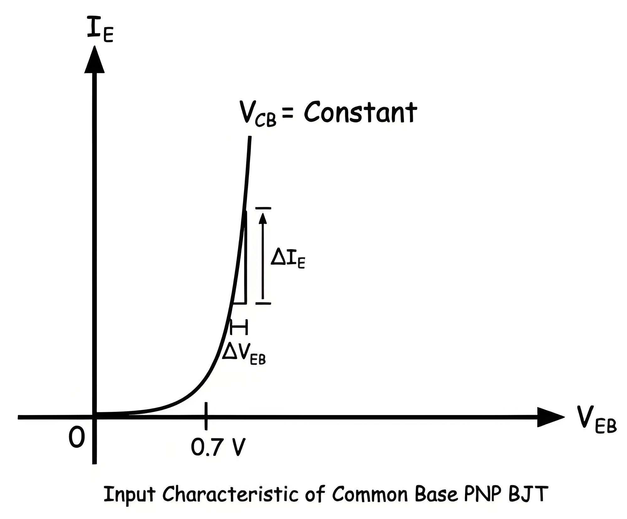
Input Characteristic
Wannan shine cikakken tufa mai girma da tufa mai girma na transistor. Tufa mai girma shine tufa mai girma (IE) da kuma tufa mai girma shine tufa mai girma (VEB). Ba a dole ne tufa mai girma (IE) ya faru da tufa mai girma (VEB) don ka ɗaukar forward barrier potential na junction base-emitter.

Resistance mai girma na circuit shine ratio of change in tufa mai girma (ΔV EB) zuwa tufa mai girma (ΔIE) a cikin voltage constant collector-base (VCB = Constant). Saboda tufa mai girma (ΔIE >> ΔVEB), resistance mai girma na common base transistor shine mai tsawo.

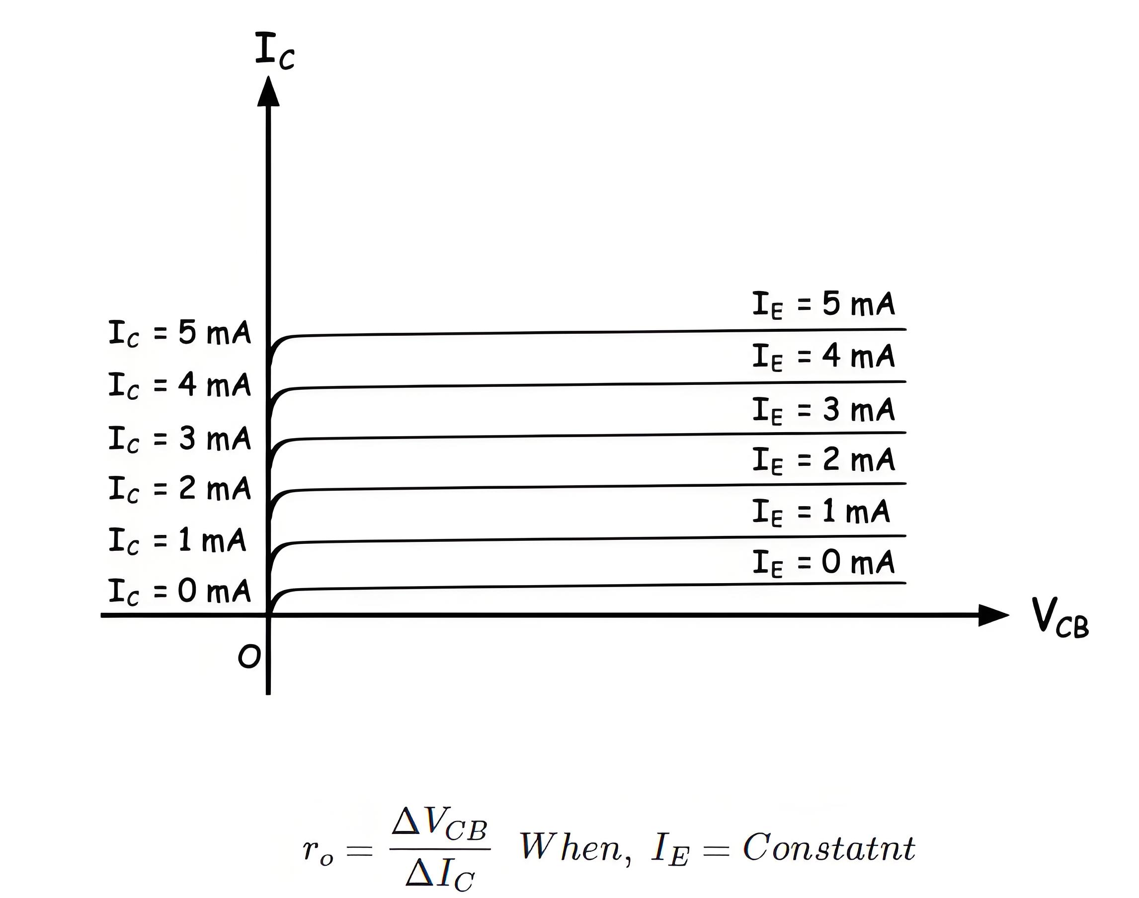
Output Characteristic
Tufa mai fitarwa ya zama constant value idan an haɗa reverse biased daɗi a cikin tufa mai girma da tufa mai fitarwa. Saboda haka, tufa mai fitarwa ya zama da ci gaba a cikin tufa mai fitarwa a lokacin da voltage na tufa mai fitarwa ya zama mai tsawo. Amma a cikin voltage mai yawa, junction base-collector ya zama da reverse biased daɗi, kuma tufa mai fitarwa ya zama constant for a certain tufa mai girma, kuma ya zama da tufa mai girma kawai.
A cikin wannan halin, duk tufa mai girma, ba tufa mai girma, ya zama tufa mai fitarwa. Saboda tufa mai fitarwa ya zama constant for the specified tufa mai girma a cikin wannan region, increase of tufa mai fitarwa ya zama mai tsawo compared to the increase of tufa mai fitarwa.
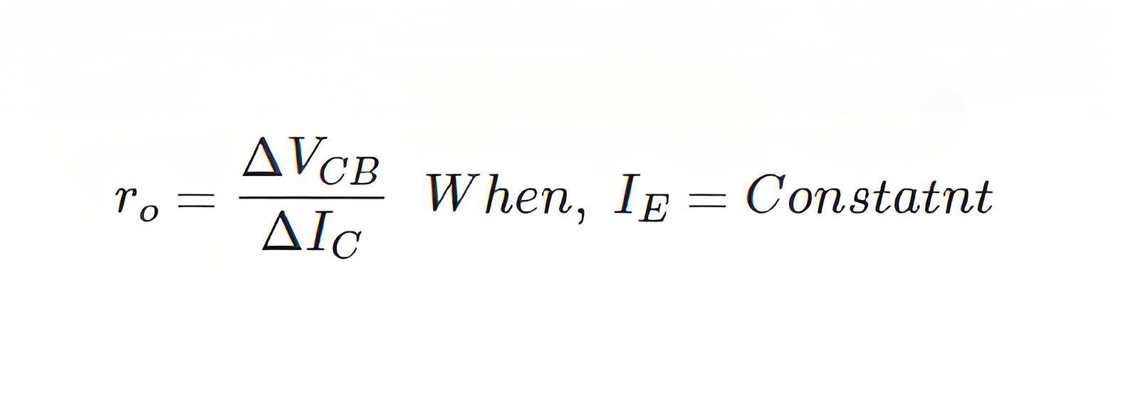
Ratio of change in tufa mai fitarwa zuwa change in tufa mai fitarwa shine output resistance of common base mode of a transistor. Naturally, the value of output resistance is very high in the common base mode of a transistor.

Common Emitter Connection of BJT
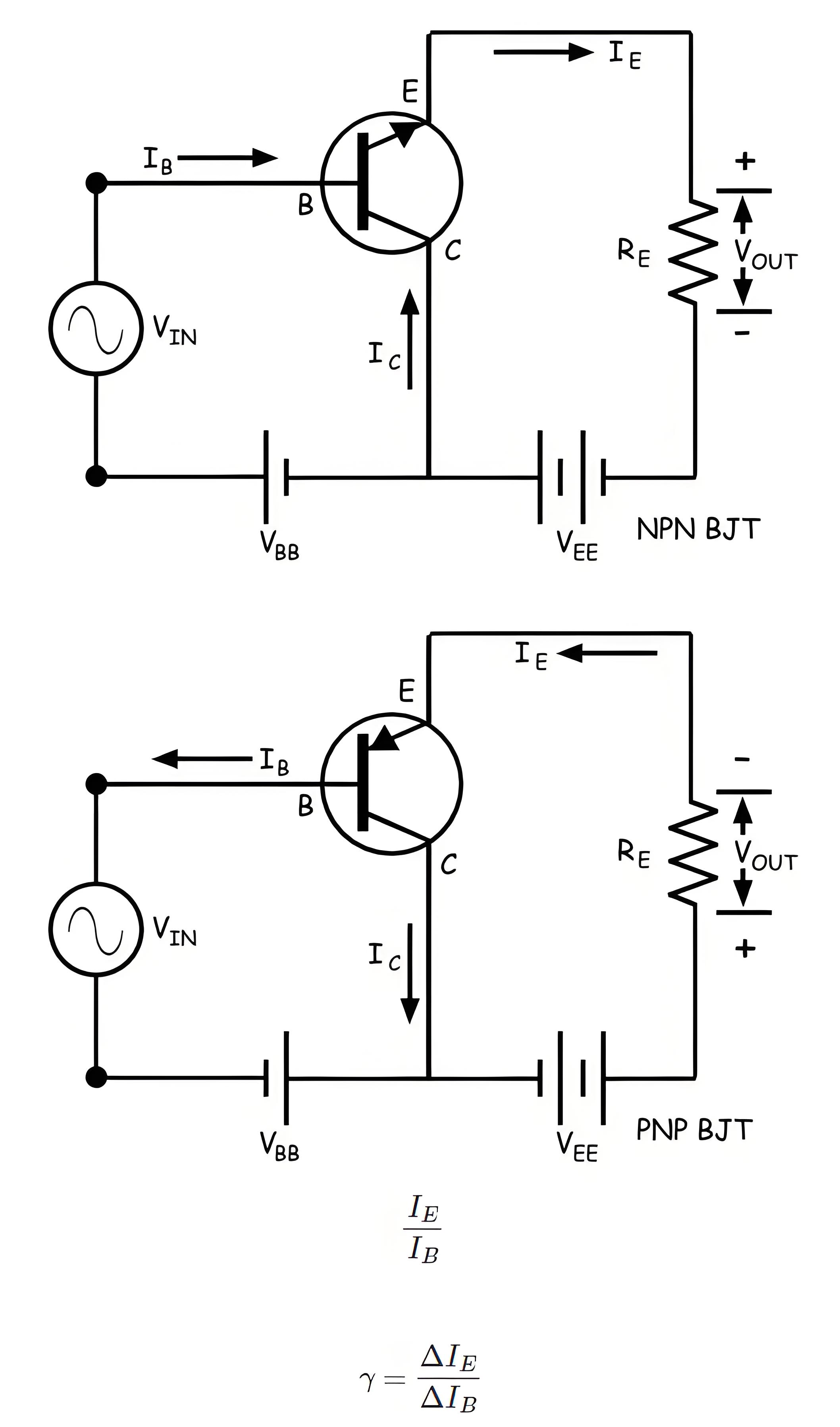
Common Emitter Transistor shine transistor connection da ake amfani da shi a mafi yawan lokaci. A nan tufa mai girma shine tufa mai girma ga sabon tufa da tufa na fitarwa. Circuit connected between tufa mai girma da tufa mai girma shine tufa mai girma, da kuma circuit connected between tufa mai fitarwa da tufa mai girma shine tufa mai fitarwa. Common emitter mode na npn transistor da pnp transistor suna nufin cewa an samu a cikin hotunan da ake bayyana a nan.

Current Gain
In common emitter configuration, the input current is base current (IB) and the output current is collector current (IC). In bipolar junction transistor, the base current controls the collector current. The ratio of change in collector current (ΔIC) to change in base current (ΔIB) is defined as the current gain of common emitter transistor. In a bipolar junction transistor, the emitter current (IE) is the sum of the base current (IB) and collector current (IC). If base current changes, the collector current also changes and as a result the emitter current gets also changed accordingly.
Again the ratio of change of collector current to the corresponding change in emitter current is denoted by αAs the value of base current is quite low compared to the collector current (IB << IC), the current gain in a common emitter transistor is quite high and it ranges from 20 to 500.

Characteristic of Common Emitter Transistor
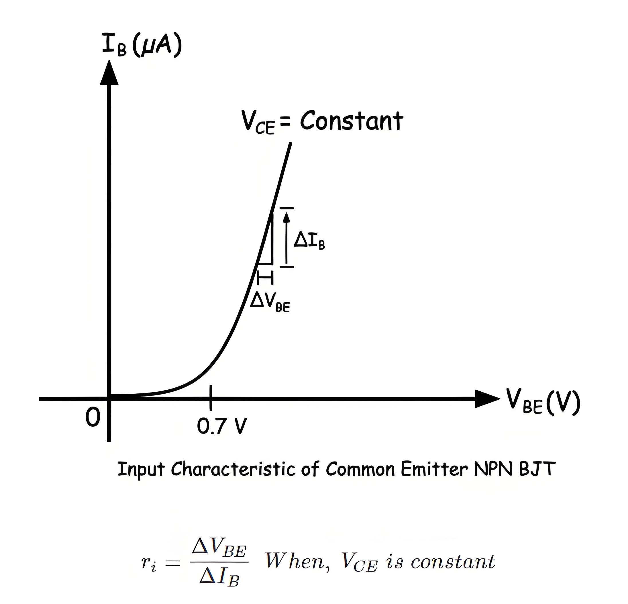
In common emitter mode of the transistor, there are two circuits – input circuit and the output circuit. In the input circuit, the parameters are base current and base-emitter voltage. The characteristic curve drawn against variations of base current and base-emitter voltage is input characteristic of a common emitter transistor. The pn junction between base and emitter is forward biased hence the characteristic would be similar to that of a forward biased pn junction diode. Here also the base current does not get any value before the base-emitter voltage crosses the forward barrier potential of the junction but after that, the base current rises significantly with the increase of base-emitter voltage. The rate of rising of base current with respect to the base-emitter voltage is high here but not as high as in the case of common base mode.
Hence input resistance of the circuit is higher than that of the common base mode of a transistor.

Output Characteristic of Common Emitter Transistor
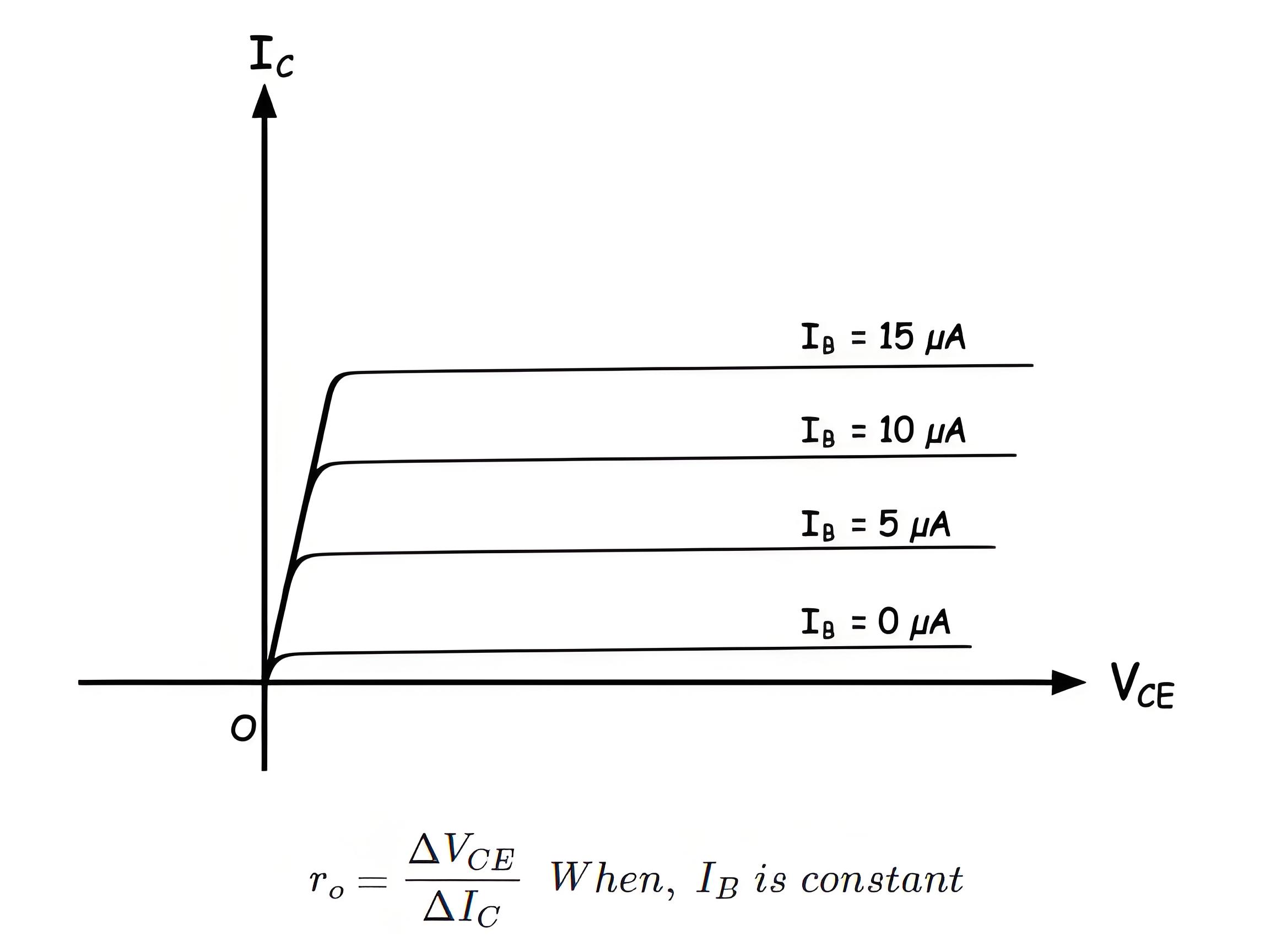
The output characteristic is drawn against variations of output current and the output voltage of the transistor. The collector current is output current and collector-emitter voltage is the output voltage of the transistor. Here the variation of collector current for different values of collector-base voltage is plotted against a fixed value of base current. It is found that at the beginning the collector current proportionately gets increased with increasing collector-emitter voltage but after certain voltage level, the collector current becomes almost constant. This is because at the beginning the base-collector junction does not get sufficient reverse biasing but after a certain voltage it becomes sufficiently reverse biased and then the major portion of charge carriers coming from emitter region to base region would migrate to collector region to contribute collector current. The number of majority carriers coming from emitter region depends on the base current in a BJT hence for a specific base current the collector current is constant.
The output resistance would be

Common Collector Connection of BJT
In common collector configuration the input circuit is between base and collector terminal and the output circuit is between emitter and collector terminal.
The ratio of change of emitter current to change of base current is defined as the current gain of common collector configuration. This is denoted as,
The current amplification factor of the circuit is the ratio of change of emitter current to change of base current when a time-varying signal is applied to the input.

Input Characteristic of Common Collector Transistor
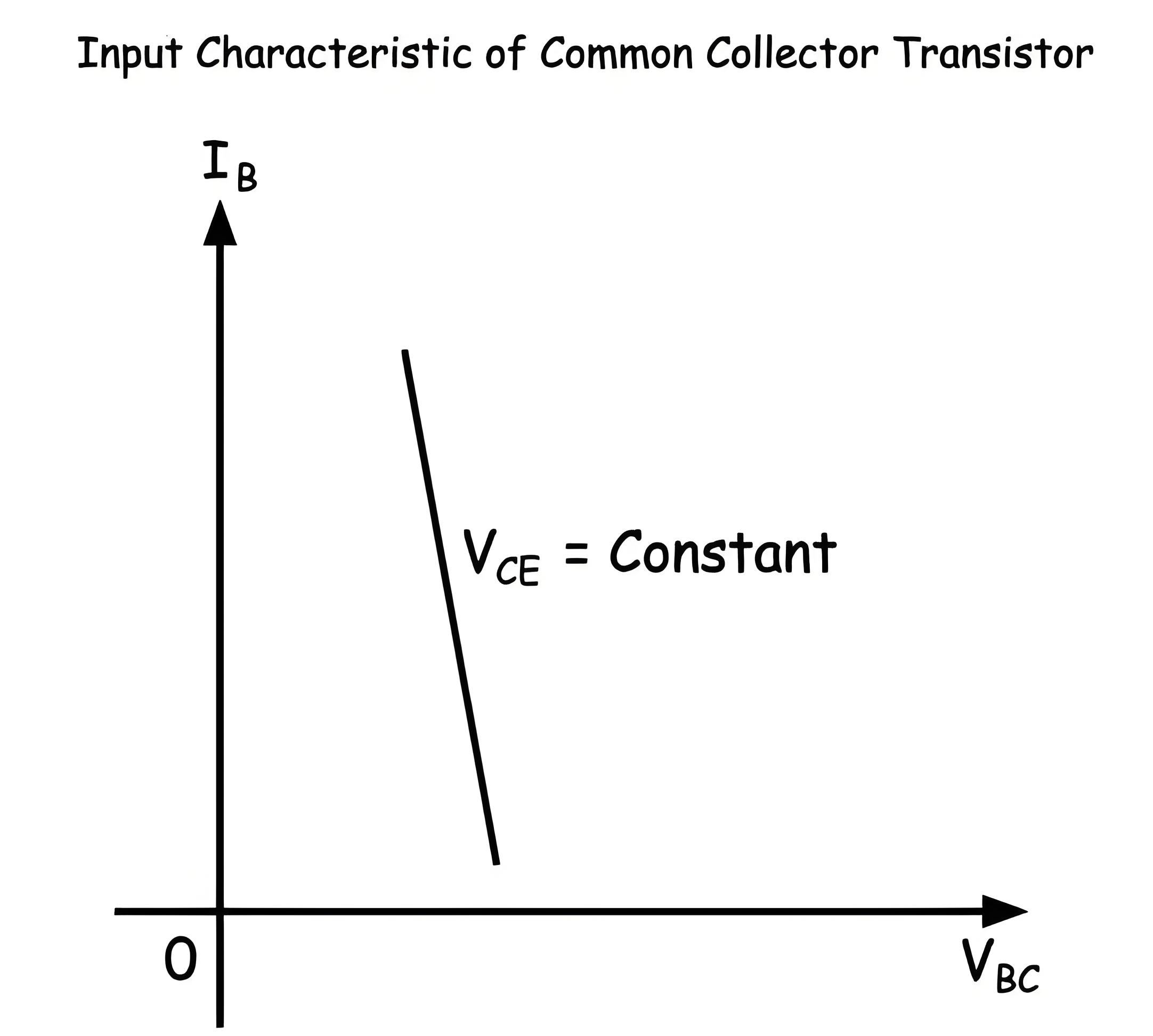
The input current is base current and input voltage of the transistor is base-collector voltage. The base-collector junction is reverse biased and hence with increasing base-collector voltage the reverse biasing of the junction increases. This causes base current to decrease slightly with the increase in base-collector voltage. Since at this condition more minority carriers of the base region will propagate to collector region and hence electron-hole recombination rate would get decreased in the base region causing a decrement in base current.

Output Characteristic of Common Collector Transistor
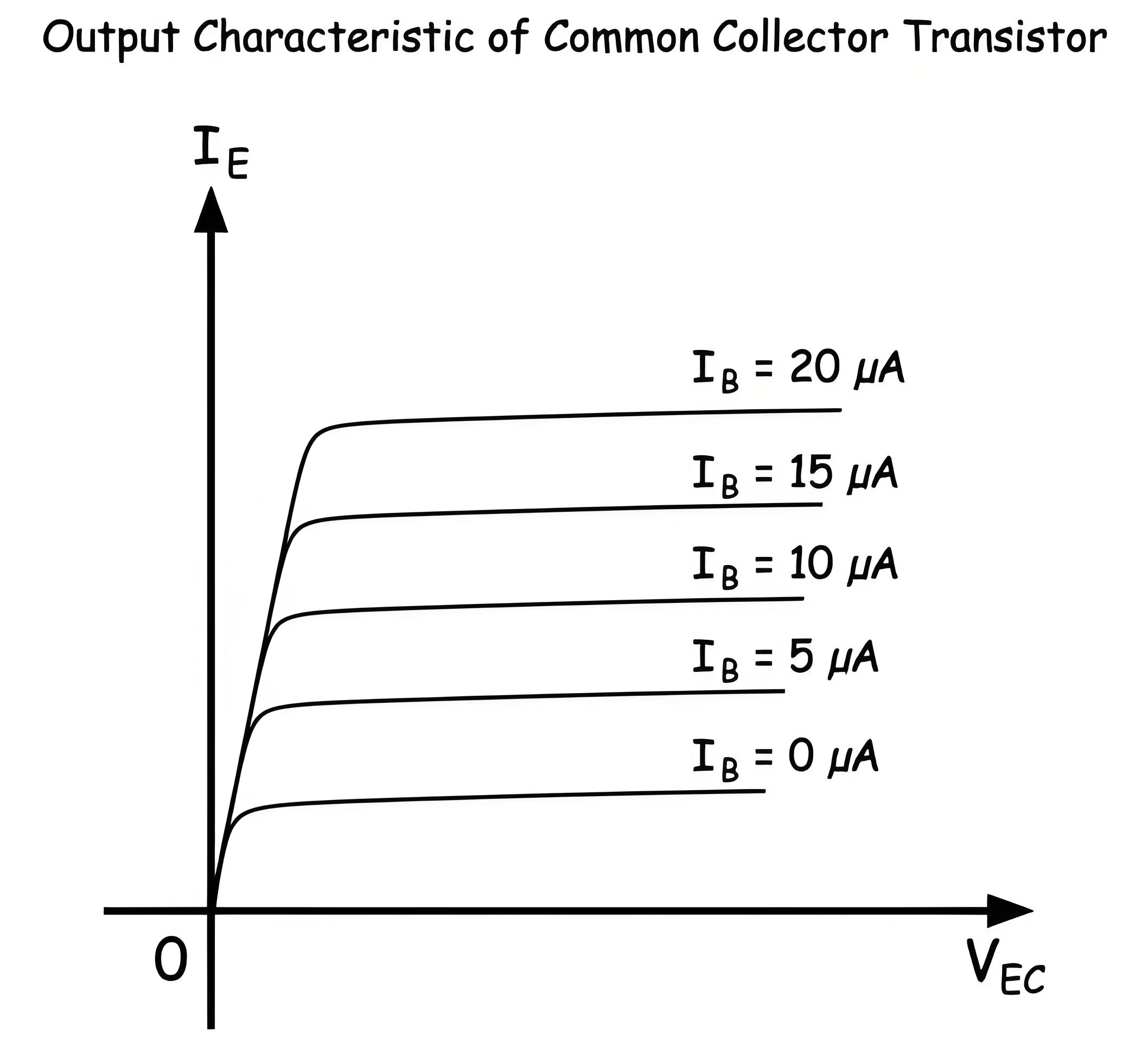
The output characteristic of a common collector transistor is nearly the same as the output characteristic of a common emitter transistor. The only difference that here in the case of common collector configuration the output current is emitter current instead of collector current as in the case of common emitter configuration. Here also for a fixed base current, the emitter current increases linearly with increasing collector-emitter voltage up to a certain level of this voltage and then the emitter current gets almost constant irrespective of collector-emitter voltage. Although there would be a very slow increase of emitter current with the collector-emitter voltage as shown in the characteristic curve below.
