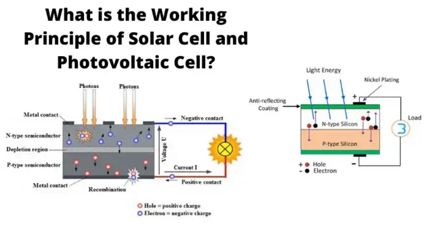
Rêzikîn dijimêr bêtiriyê bi rêzikî elektrîk biguhezîne ye ku li ser fenomenek da ku navê wê photovoltaic effect e. Heta çi ke materialên semiconductorkan derbarê reyê rojan hene, yek ji fononên reyê rojan hatine wergerandin lê krisalên semiconductorkan, ku hûn dikarin taybetmendîyi pir zêde ya elektronên azad di krisal de pike. Ev ê amarê bêtirin e ku elektrik bi rêzikî photovoltaic effect dagihînin. Photovoltaic cell an jî unita bêtirin e cihazê ku di wan de photovoltaic effect bikar înin tuhaf elektrik ji rêzikî rojan biguhezîne. Silisium an jî materiala semiconductorka herî zişt bi karîne ji bo inasîna photovoltaic cell. Atom silisium gotinên valenceya çar hene. Di kristalê tevda de, har atom silisium gotinên valenceya çar yake bi atom silisium dinikinîn digelînewe, ku nîşana covalent bond ne. Bi vê şêwe, kristal silisium strukturê tetrahedral lattice peyda kir. Heke reyê rojan li ser materialên herî dest be, yek berd reyê rojan reflektandin, yek berd transmittandin, û yek berd absorbindin.
Sedemek dersmi hate ku heke reyê rojan li ser kristal silisium dest be. Eger intensivî reyê rojanê piştguh be, gotinên fononên berd hatine wergerandin lê kristal, û fononên wergerandî yên ev dikarin gotinên electronên covalent bond bike. Electronên excite yên ev dikarin energiya bêkêşin bi karîne ji band valence bandê conduction bidevin. Ji ber ku levela energiya electronên ev di band conduction de, hûn ji covalent bond derkevin û hole ên band de wergerin. Elektronên azad yên ev dikarin bi şêwe random di strukturê kristal silisium de here bike. Elektronên azad û hole'yan ên di photovoltaic cell de roleya vital dikin. Elektronên û hole'yan û hûn dikarin namekirin light-generated electrons and holes. Elektronên û hole'yan yên light generated tune elektrik di kristal silisium de nebiguhezînin. Divê mechanisma bêtirî bihêzi bide.
Heke impurity pentavalent wek phosphorus bi silisium zêde bike, gotinên valenceya çar yekê yek yek bi atomên silisium neighbor bi covalent bonds share bikin, û gotinên valenceya penhemî nebeşk ji bo inasîna covalent bond.
Gotinên penhemî yek yek bi atom parentakî li ser silisium loose bounded be. Jî ber temperaturê oda, energiya thermal di kristal de piştguh be ku disassociate yek yek loose fifth electron ji atom parent phosphorus bikin. Gotinên penhemî yek yek disassociated ji atom parent phosphorus be, atom phosphorus positive ions immobile bike. Disassociated electron free bike, lê nebeşk ji bo incomplete covalent bond û hole di kristal de re-associated be. Elektronên azad yên bi pentavalent impurity hatine wergerin herî ready ne bi karîne current conduct di semiconductor de. Herî bi elektronên azad, ew materyala electrically neutral e, ji ber ku number of positive phosphorous ions locked inside the crystal structure exactly equal to the number of the free electrons come out from them. Process of inserting impurities in the semiconductor known as doping, and the impurities are doped are known as dopants. Pentavalent dopants which donate their fifth free electron to the semiconductor crystal are known as donors. Semiconductors doped by donor impurities are known as n-type or negative type semiconductor as there are plenty of free electrons which are negatively charged by nature.
Heke instead pentavalent phosphorous atoms, trivalent impurity atoms like boron are added to a semiconductor crystal opposite type of semiconductor will be created. In this case, some silicon atoms in the crystal lattice will be replaced by boron atoms, in other words, the boron atoms will occupy the positions of replaced silicon atoms in the lattice structure. Three valance electrons of boron atom will pair with valance electron of three neighbour silicon atoms to create three complete covalent bonds. For this configuration, there will be a silicon atom for each boron atom, fourth valence electron of which will not find any neighbour valance electrons to complete its fourth covalent bond. Hence this fourth valence electron of these silicon atoms remains unpaired and behaves as incomplete bond. So there will be lack of one electron in the incomplete bond, and hence an incomplete bond always attracts electron to fulfil this lack. As such, there is a vacancy for the electron to sit.
This vacancy is conceptually called positive hole. In a trivalent impurity doped semiconductor, a significant number of covalent bonds are continually broken to complete other incomplete covalent bonds. When one bond is broken one hole is created in it. When one bond is completed, the hole in it disappears. In this way, one hole appears to disappear another neighbour hole. As such holes are having relative motion inside the semiconductor crystal. In the view of that, it can be said holes also can move freely as free electrons inside semiconductor crystal. As each of the holes can accept an electron, the trivalent impurities are known as acceptor dopants and the semiconductors doped with acceptor dopants are known as p-type or positive type semiconductor.
In n-type semiconductor mainly the free electrons carry negative charge and in p-type semiconductor mainly the holes in turn carry positive charge therefore free electrons in n-type semiconductor and free holes in p-type semiconductor are called majority carrier in n-type semiconductor and p-type semiconductor respectively.
There is always a potential barrier between n-type and p-type material. This potential barrier is essential for working of a photovoltaic or solar cell. While n-type semiconductor and p-type semiconductor contact each other, the free electrons near to the contact surface of n-type semiconductor get plenty of adjacent holes of p-type material. Hence free electrons in n-type semiconductor near to its contact surface jump to the adjacent holes of p-type material to recombine. Not only free electrons, but valence electrons of n-type material near the contact surface also come out from the covalent bond and recombine with more nearby holes in the p-type semiconductor. As the covalent bonds are broken, there will be a number of holes created in the n-type material near the contact surface. Hence, near contact zone, the holes in the p-type materials disappear due to recombination on the other hand holes appear in the n-type material near same contact zone. This is as such equivalent to the migration of holes from p-type to the n-type semiconductor. So as soon as one n-type semiconductor and one p-type semiconductor come into contact the electrons from n-type will transfer to p-type and holes from p-type will transfer to n-type. The process is very fast but does not continue forever. After some instant, there will be a layer of negative charge (excess electrons) in the p-type semiconductor adjacent to the contact along the contact surface. Similarly, there will be a layer of positive charge (positive ions) in the n-type semiconductor adjacent to contact along the contact surface. The thickness of these negative and positive charge layer increases up to a certain extent, but after that, no more electrons will migrate from n-type semiconductor to p-type semiconductor. This is because, while any electron of n-type semiconductor tries to migrate over p-type semiconductor it faces a sufficiently thick layer of positive ions in n-type semiconductor itself where it will drop without crossing it. Similarly, holes will no more migrate to n-type semiconductor from p-type. The holes when trying to cross the negative layer in p-type semiconductor these will recombine with electrons and no more movement toward n-type region.
In other words, negative charge layer in the p-type side and positive charge layer in n-type side together form a barrier which opposes migration of charge carriers from its one side to other. Similarly, holes in the p-type region are held back from entering the n-type region. Due to positive and negative charged layer, there will be an electric field across the region and this region is called depletion layer.
Now let us come to the silicon crystal. When light ray strikes on the crystal, some portion of the light is absorbed by the crystal, and consequently, some of the valence electrons are excited and come out from the covalent bond resulting free electron-hole pairs.
If light strikes on n-type semiconductor the electrons from such light-generated electron-hole pairs are unable to migrate to the p-region since they are not able to cross the potential barrier due to the repulsion of an electric field across depletion layer. At the same time, the light-generated holes cross the depletion region due to the attraction of electric field of depletion layer where they recombine with electrons, and then the lack of electrons here is compensated by valence electrons of p-region, and this makes as many numbers of holes in the p-region. As such light generated holes are shifted to the p-region where they are trapped because once they come to the p-region cannot be able to come back to n-type region due to the repulsion of potential barrier.
As the negative charge (light generated electrons) is trapped in one side and positive charge (light generated holes) is trapped in opposite side of a cell, there will be a potential difference between these two sides of the cell. This potential difference is typically 0.5 V. This is how a photovoltaic cells or solar cells produce potential difference.
Statement: Respect the original, good articles worth sharing, if there is infringement please contact delete.


