1 Hardware Design of Tester Power Supply
This device uses a standard small - signal generating device to generate small - current signals with the required frequency and phase angle. Then, through the amplifying circuit and phase - modulating circuit, the working power supply is generated.
1.1 Power Frequency Sine Wave Small - Current Signal Generating Device
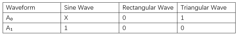
The sine wave generating circuit is mainly composed of the waveform generating chip MAX038 produced by MAXIM Corporation of the United States. According to the test requirements, this circuit needs 3 chips and can generate at least 3 - channel sine signals. MAX038 is a high - frequency precision function generator. By building a simple peripheral circuit (see Figure 1) and controlling the chip pins A₀ and A₁ (see Table 1), sine waves, rectangular waves and triangular waves can be generated.
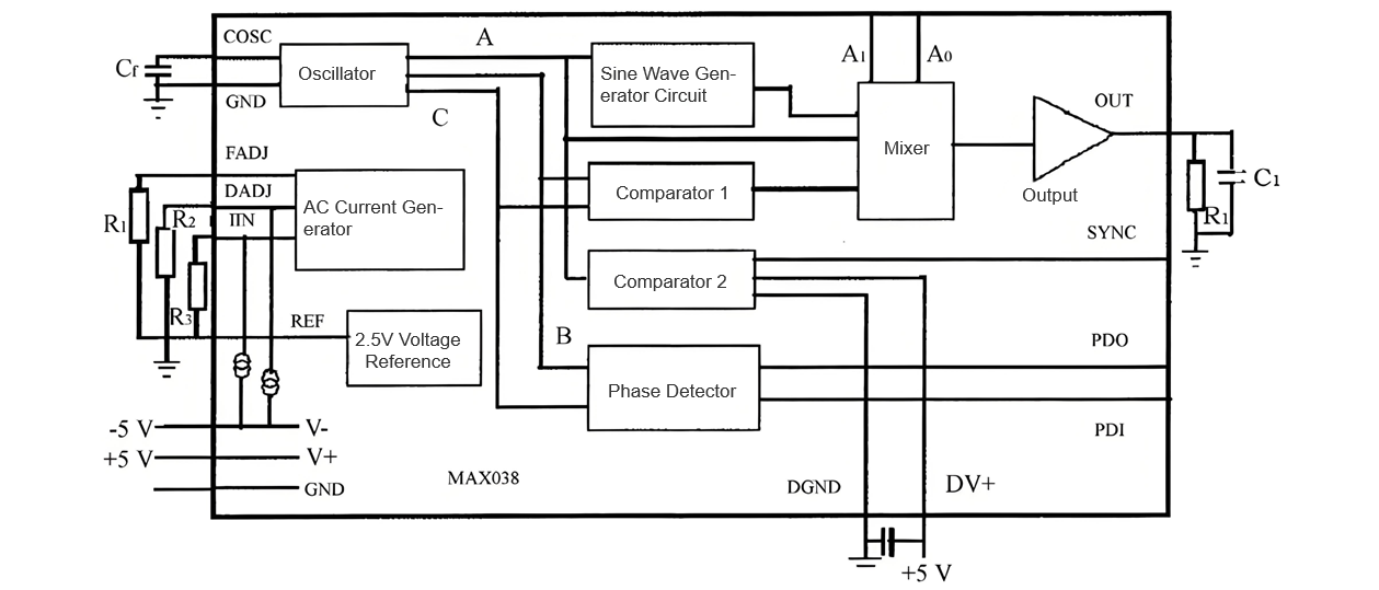
Frequency adjustment: When the pin FADJ is at zero level, the output frequency can be calculated by the formula Fₐ = IIN / Cf(where IIN= Vref/ Rin; Fₐ is the output frequency, in MHz; Cf is the external circuit capacitance of the oscillator, in pF; IIN is the output current of pin IN, in μA; Vref is the output voltage of pin REF; Rin is the input resistance of pin IN).
Duty cycle adjustment: The voltage change of pin DADJ will change the relative charging and discharging rates of capacitor Cf. When pin DADJ is at zero level, the duty cycle is 50%. When the voltage of pin DADJ changes in the range of -2.3~2.3 V, the duty cycle changes in the range of 85%~15%. The duty cycle adjustment can be calculated by the formula Vdadj =₋50%- DC×0.0575 (where Vdadj is the voltage on pin DADJ).
1.2 Realization of Single - phase, Three - phase and Two - phase Orthogonal Output of Small - current Signals
The phase detector inside MAX038 can be used to construct a phase - locked loop circuit. When three - phase rectangular wave signals are input to the PDI terminals of three MAX038s, the three sine wave signals output by them will be three - phase AC signals. For single - phase signal output, two sine wave signal generators can be turned off, and only the third sine wave generator works.
There is no need to input phase adjustment signals to PDI. The principle of two - phase orthogonal signal output is consistent with that of three - phase output. First, turn off one sine wave signal generator, and then apply two orthogonal rectangular wave signals to the PDI terminals of the remaining two sine wave signal generators respectively. The two sine wave signals output by them will be two - phase orthogonal AC signals. This rectangular external synchronization signal is implemented by a programmable PLD. Divide the three - phase power - frequency square wave signal into 6 states (see Figure 2).
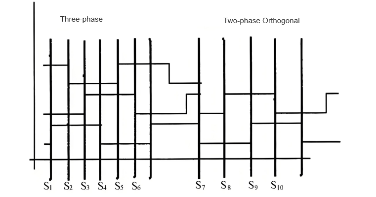
Obviously, the time difference between each state is 3.3 ms (with a period of 20 ms at 50 Hz). As long as the 6 output states each last for 3.3 ms and cycle infinitely in the positive sequence, the power - frequency three - phase square wave signal can be output. Similarly, process the two - phase orthogonal signal and divide it into 4 states (S₇, S₈, S₉, S₁₀). The time difference between each state is 5 ms. As long as the 4 output states each last for 5 ms and cycle infinitely in the positive sequence, the power - frequency two - phase orthogonal square wave signal can be output.
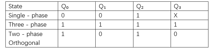
The phase synchronization control waveform of MAX038 outputs signals Q₂, Q₀, Q₁ from pins 16#, 14#, and 13# of the P16R6 programmable chip (refer to the P16R6 data) to the external synchronization signal PDI terminals of three MAX038s. An AND gate is set at the output of pin 13#, controlled by signal Q₃. By editing the program to make Q₀, Q₁, Q₂, Q₃ meet specific conditions (Table 2), the generation of three - phase and two - phase orthogonal rectangular external synchronization signals can be achieved
1.3 Implementation Principle of Power Amplification
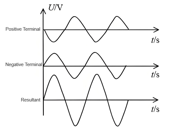
The single - phase amplification circuit is designed as a Bridge - Tied Load (BTL) structure. The two ends of the load are respectively connected to the output terminals of two amplifiers. The output of one amplifier is the mirror output of the other. That is, the signals loaded on the two ends of the load only have a phase difference of 180°. The voltage obtained on the load is twice the original single - ended output voltage (see Figure 3), meeting the requirement that the single - phase output is not less than 100 W.
2 Debugging of the Tester Power Supply Hardware
2.1 Distortion Adjustment of Output Waveform
Duty cycle setting: Apply a voltage control signal ranging from -2.3V to +2.3V to the DADJ terminal of MAX038 to adjust the charging and discharging time of capacitor Cf. Adjust the triangular wave output by the oscillator within the range of 10% - 90%, and finally generate distorted sine waves, sawtooth waves, and pulse waves. Since a constant current of 250 μA flows into the DADJ terminal, connect a resistor Rd between this terminal and the reference power supply pin REF. Then: Vdadj = Vref - 0.25Rd; Adjusting the value of Rd can adjust the duty cycle of triangular waves and sawtooth waves without affecting the synchronous output pulses, and Rd should not be greater than 20 kΩ.
2.2 Frequency Adjustment of Output Waveform
MAX038's output frequency is controlled by oscillation capacitor Cf, IIN current, and FADJ voltage. With a fixed Cf, fine frequency tuning is achieved by controlling the IIN pin. For digital control, DACs are connected to IIN and FADJ. These generate small voltages, converted to 0-748 μA current (plus 2 μA from the network) for 2-750 μA at IIN, creating the output frequency range. The DAC divides this range into 256 steps, enabling coarse adjustment via IIN current and fine tuning through the DAC.
2.3 Voltage Output Adjustment of Power Amplification Circuit
The three single-phase step-up transformer circuits function as a three-phase transformer for simultaneous signal boosting (avoiding the significant impact of direct three-phase transformer use on small signals). Voltage adjustments between 200 V and 80 V are achieved by regulating the transformers.
2.4 DC Working Circuit Voltage Adjustment
A DC voltage transformation and stabilization circuit provides stable DC power from the on-site 220 V AC supply. It outputs +35 V and +5 V (meeting transformer precision requirements) using 7805 and 7905 DC power modules.
3 Conclusion
The designed power supply features clear functionality, cost-effectiveness, and high output precision, fully meeting testing instrument requirements.
Modular design reduces complexity, with interconnected yet independent circuits. Clear functional division (sine wave generation, phase control, power amplification, DC supply) allows continuous upgrades to meet user needs.
Control signals Q0-Q3 enable MCU compatibility and digital control. Combined with modular design, the device outputs three-phase, two-phase orthogonal, and single-frequency sine signals, plus rectangular/triangular waves with various phase requirements, satisfying diverse tasks.